
Circuit Diagram
Index 725
DUAL_OUTPUT_500_kHz±15_V_DC_TO_DC_CONVERTER
Published:2009/7/13 2:11:00 Author:May

The LT1371 dual-output flyback converter circuit shown generates ±15 V at 200 mA each from a 5-V supply. The LT1371 is a 500-kHz high-efficiency switching regulator with 3-A power switch, yet it uses only 4 rnA typical quiescent current. The high operating frequency allows a small surfacemount, dual-output winding flyback transformer to be used. Each output is monitored by separate positive and negative feedback inputs on the LT1371 to be sure that neither output rises above its set point. This removes a common problem in dual-output designs using a single controller: the tendency of the voltage of the least loaded output to fly high. Output voltage regulation is best when both outputs are evenly loaded. (View)
View full Circuit Diagram | Comments | Reading(3029)
Adjustable regulated power supply circuit with heavy current
Published:2011/7/19 10:04:00 Author:Nancy | Keyword: Adjustable regulated power supply, heavy current
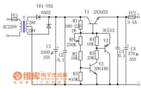
The regulated power supply is adjustable between the range of 3.5V to 25V, the current is heavy and it adopts adjustable regulating transistor circuit to obtain satisfied and stable voltage.
Working principle: The DC voltage is provided to the base of regulating transistor by R1 after filtered and rectified, which makes regulating transistor conduct, and when V1 conducts, the voltage across RP, R2 make V2 conduct. The emitter and collector voltage of V1,V2 and V3 don't change any longer (the function is as same as the regulating transistor). You can obtain stable output voltage by adjusting RP, the ratio of R1, RP, R2 and R3 decides the value of output voltage of the circuit. (View)
View full Circuit Diagram | Comments | Reading(2372)
CLAMP_AMPLIFIER
Published:2009/7/13 2:11:00 Author:May
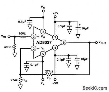
A clamp amplifier is a limiting or bounding circuit. For input voltages between two levels, VH and VL, the output is proportional to the input. For inputs greater than VH or less than VL (VH or VL × the amplifier gain, AV), irrespective of the input. The threshold voltages, VH and VL, can be fixed or variable. If the amplifier can handle positive and negative input/output voltages, VH and VL can have any positive or negative value within the specified range, as long as VH > VL. (View)
View full Circuit Diagram | Comments | Reading(940)
3_TO_7_V_DC_TO_DC_CONVERTER
Published:2009/7/13 2:09:00 Author:May

Converting the voltage from a four-cell battery pack to 5 V while using the full capacity of the batteries requires two modes of operation: step-down from an input voltage of 6 V and step-up from an input of 4 V (or less). A flyback topology can accomplish this, but uses a costly custom transformer. The LT1300 circuit shown utilizes the simple SEPIC topology, and is capable of 220 mA of output current at 5 V from a minimum 3-V input. The two inductors specified are available off the shelf. The circuit uses a boost section and a buck, or step-down, section, with the two inductors (L1 and L2) and two capacitors (C2 and C3) all acting as energy-storage elements. Efficiency is slightly less than that of a direct step up (see graph), but is better than that of an equivalent flyback configuration. Other features of the circuit include shutdown (10 μA max. supply current) with full input-to-output isolation, which allows the output to go to zero volts, yet present no load to the batteries.Also, either a 3.3-V or 5-V output can be selected by using the logic-select pin of the LT1300. (View)
View full Circuit Diagram | Comments | Reading(1130)
PROGRAMMABLE_AMPLIFIER
Published:2009/7/13 2:07:00 Author:May

The programmable gain amplifier (PGA) is ideal for applications, such as data loggers and automatic measuring instruments. The amplification can be set anywhere between unity and ×1000. The bandwidth at any amplification is >30 kHz. The current drain does not exceed 7 mA. The input signal is buffered by IC1a and then applied to amplifier IC1b. The amplification of this stage depends on how feedback resistors R5 to R8 are switched into the circuit by IC2. How the resistors are inter-coupled depends on the logic levels at inputs A and B. The interrelation among the resistors, the total amplification, and the logic levels is shown in the table. After the output signal of IC1b has passed through the multiplexer, it is applied at ×100 amplifier IC1d via buffer IC1c. The overall amplification is set with logic levels at inputs A and B as shown in the table. The amplification of the first stage has been kept low purposely to ensure that the value of the feedback resistor does not have to be high, which makes the effect of the leakage current of the multiplexer negligible. (View)
View full Circuit Diagram | Comments | Reading(0)
OP_AMP_ERROR_CURRENT_MEASUREMENT_CIRCUIT
Published:2009/7/13 2:07:00 Author:May
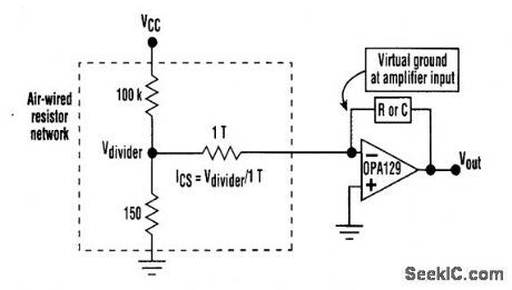
Using an air-wired resistor-divider network, designers can make a precision femtoampere source that can inject a known error current into the amplifier to check the circuit's accuracy. (View)
View full Circuit Diagram | Comments | Reading(971)
9_V_DC_TO_DC_CONVERTER
Published:2009/7/13 2:06:00 Author:May


In portable applications, 9-V batteries are frequently used. For low-power dc-to-dc step-down conversion, the LTC1174 is a simple integrated solution. With its internal MOSFET power switch, the LTC1174-5 requires only four extemal parts to achieve 90-percent efficiency. All surface-mount assembly is standard, with high-frequency operation at up to a 200 kHz switching frequency. Extremely low dropout operation is possible because the LTC1174 operates at 100-percent duty cycle with low input voltages. A single logic-level input selects an output voltage of 3.3 V or 5 V. (View)
View full Circuit Diagram | Comments | Reading(1164)
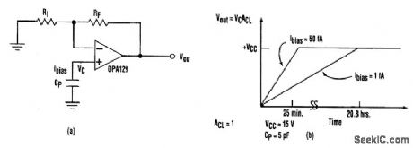
OP_AMP_ERROR_SOURCE_CIRCUIT
Published:2009/7/13 2:06:00 Author:May

The basic error sources for an op amp are shown referenced to the output. In high-source-imbecome quite dominant. pedance applications, the input bias current terms can become quite dominant. (View)
View full Circuit Diagram | Comments | Reading(737)
OP_AMP_BIAS_PRECAUTION_CIRCUIT
Published:2009/7/13 2:05:00 Author:May
All amplifiers must have a dc path for input-bias current to return to ground (a). Without this path, an amplifier will eventually drift to the output rail (b). (View)
View full Circuit Diagram | Comments | Reading(661)
COMPRESSION_AMPLIFIER
Published:2009/7/13 2:04:00 Author:May
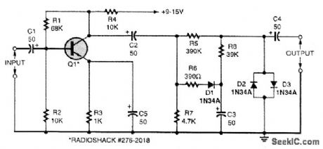
Here's a compression-type amplifier that can be used to keep the volume level of an organ constant. Unlike compressors used for public-addr ess-system applications, the organ leveler can respond to the entire range of frequencies generated by the organ without-coloring the voice. It can handle large fluctuations in input signal without clippinl. It also works well as a microphone leveler (View)
View full Circuit Diagram | Comments | Reading(2188)
LONG_DELAY_555_MONO
Published:2009/7/13 2:04:00 Author:May
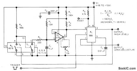
FET-input 3140 opamp is used to multiply effective values of timing components Rt and Ct, eliminating need for high-value precision resistor and large low-leakage capadtor. Combination performs as standard 555 mono except that timing equation is T = 100RtCt (for condition wherein division resistors R1 and R2 are chosen for 91-to-1 operation). Circuit has uncommitted open-collector output from pin 7 of 555, which can be referred to any voltage from 0 to + 15 V. Pin 4 is between pins 6 and 8 on 555.-W. G. Jung, Take a Fresh Look at New IC Timer Applications, EDN Magazine, March 20 1977, p 127-135. (View)
View full Circuit Diagram | Comments | Reading(1405)
WIDER_BANDWIDTH_PHOTODIODE_AMPLIFIER
Published:2009/7/13 2:03:00 Author:May

Many photodiode applications require high gain and wide bandwidth. A dc-restored photodiode amplifier (Fig. 1) is useful in situations where a time-varying light signal of interest competes with unwanted ambient background light. To extend the amplifier's bandwidth, the design can be modified to provide current-to-voltage conversion with subsequent voltage gain (Fig. 2). Current from the low-capacitance photodiode flows through Rg and establishes a voltage at the noninverting terminal. This voltage then receives a gain equal to 11Rf/R1. With the values shown in Fig. 2, the equivalent transimpedance Rg(11Rf/R1) is equal to 10Ω. The design uses an invertingintegrator to drive a restoration current through Rg This low-frequency current cancels current from the photodiode at frequencies below the low-frequency cutoff pole. The low-frequency pole in Fig. 2 is given by f-3dB5 (1/2πRC) (11Rf/R1). For the values shown, this is equal to 159 Hz. Rg helps determine the equivalent transimpedance and provides the path for the low-frequency restoration current. The measured high-frequency cutoff for the circuit in Fig. 1 is 4.9 kHz, with a total in-bartd noise of 370 μV rms. In Fig. 2, the high-frequency cutoff is extended to 11.7 kHz, with a total in-band noise of 589 μV rms.
(View)
View full Circuit Diagram | Comments | Reading(3722)
3_min_TO_4_h
Published:2009/7/13 2:02:00 Author:May
Presettable analog timer achieves long time intervals by discharging C1 into input terminal 3 of CA3094 programmable opamp, which provides sufficient output current for driving thyristors and other control devices.- Circuit ldeas for RCA Linear ICs, RCA Solid State Division, Somerville, NJ, 1977, p 8. (View)
View full Circuit Diagram | Comments | Reading(809)
Tube stereo power amplifier circuit diagram
Published:2011/8/4 1:33:00 Author:Ecco | Keyword: Tube stereo, power amplifier

View full Circuit Diagram | Comments | Reading(1201)
5 V to 12 V booster circuit diagram
Published:2011/7/18 10:38:00 Author:Nancy | Keyword: 5 V to 12 V , booster

View full Circuit Diagram | Comments | Reading(815)
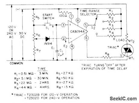
4_h_CONTROL_FOR_TRIAC
Published:2009/7/13 2:00:00 Author:May

Time at which triac is triggered by IC after momentarily pressing start switch is determined by resistor values used, When switch is released, charging capacitor C1 begins its long discharge interval. When voltage E1 becomes less than E2, pin 2 draws current and serves to reverse polarity of output at pin 6 for triggering triac. Diode limits maximum differential inputvoltage.-E. M. Noll, Linear IC Principles, Experiments, and Projects, Howard W. Sams, lndianpolls, IN, 1974, p316-317. (View)
View full Circuit Diagram | Comments | Reading(880)
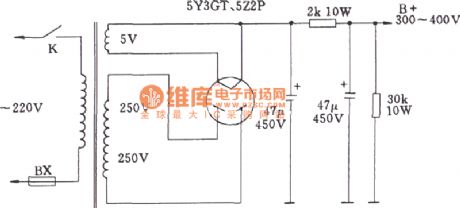
117_VAC_FROM_24_60_VDC
Published:2009/7/13 2:00:00 Author:May

Will operate from either 24- or 32-V storage battery or from 60-VDC source. Circuit shown is set up for 60-V operation. For 24/32 V, remove F1 and F4 andinsert F2 and F3, then switch S3 to 32 V. T1 is 117-V 20-A Variac with bifilar primary winding added; use 38 bifilar turns of No. 8 for 24 V and 48 turns for 32 V. Commutating capacitor C1 consists of ten 120-μF 400-VDC oil-filled capacitors (do not use electrolytics). SCRs Q1 and Q2, rated 100 A at 800 PIY (Poly Paks 92CU1167), are switched by Cornell-Dubilier 98600 60-Hz 12-V vibrator.VR1, which limits voltage across vibrator coil, consists of two 6.8-V 10-W zeners. With 60-V operation, use 1-ohm 200-W resistor in series with inverter while starting, but short it out while inverter is running. Inverter output voltage varies from 150 VAC no-load to 110 VAC with 1650-W resistive load. CR1 is 400-PIV 200-A silicon. CR2 and CR3 are 800-PIV 250-A silicon.-R. Dunaja, A High-Power SCR Inverter,QST, June 1974, p 36-37. (View)
View full Circuit Diagram | Comments | Reading(747)
Direct heating rectifier tube full-wave rectifier and filter circuit diagram
Published:2011/8/4 1:32:00 Author:Ecco | Keyword: Direct heating, rectifier tube , full-wave rectifier , filter circuit
View full Circuit Diagram | Comments | Reading(1283)
DIFFERENTIAL_AMPLIFIER
Published:2009/7/13 1:56:00 Author:May

The differential amplifier shown handles common-mode voltages up to ±24 V on a 3.3-V supply, or up to ±40 V on a 5-V supply. It is handy when interfacing analog-to-digital converters (ADCs) or data-acquisition systems (DASs) in 3.3-V or 5-V single-supply systems to inputs with a wide common-mode range. Differential amplifier X1 is the actual differential amplifier, and R1, R2, R3, and R4 are the gain-setting resistors. X2 forces the common-mode voltage at X1's inputs to zero with respect to a quiescent biasing point provided by X3. The wide availability of dual and quad low-voltage op amps permits implementations with a single IC package. Biasing at one-half supply, or at some reference well within the supply rails, is necessary because positive-going common-mode inputs require X2's output to swing negative. R5, R6, R7, and R8 should have impedance at least an order of magnitude less than the gain-setting resistors of X1. The impedance relationship of R6 and R8 to gain-setting resistors limits the use of this circuit to high-impedance differential-amplifier circuits. Therefore, it is not well suited for wide-bandwidth circuits. The high impedances also favor the use of JFET or CMOS input op amps. (View)
View full Circuit Diagram | Comments | Reading(0)
Integrated audio amplifier circuit diagram
Published:2011/8/4 1:28:00 Author:Ecco | Keyword: Integrated audio amplifier

View full Circuit Diagram | Comments | Reading(947)
| Pages:725/2234 At 20721722723724725726727728729730731732733734735736737738739740Under 20 |
Circuit Categories
power supply circuit
Amplifier Circuit
Basic Circuit
LED and Light Circuit
Sensor Circuit
Signal Processing
Electrical Equipment Circuit
Control Circuit
Remote Control Circuit
A/D-D/A Converter Circuit
Audio Circuit
Measuring and Test Circuit
Communication Circuit
Computer-Related Circuit
555 Circuit
Automotive Circuit
Repairing Circuit