
Circuit Diagram
Index 723
DECIBEL_METER
Published:2009/7/16 4:50:00 Author:Jessie

The circuit consists essentially of IC1, the CA3089E, a 0-to 100-μA meter M1, on-off switch S1, a few resistors and capacitors, and a diode. The graph shows the plot of dc volts out of METER OUT, pin 13 of IC1 (33 kΩ to ground), vs. the input signal in microvolts on IF IN 1, pin converted to decibels above 1 mW. IC1 detects the signal level and generates a nearly logarithmic dc output. To linearize the high end of this curve, diode D1 and resistor R6 shunt some of the dc as the voltage on pin 13 rises above 3 V. The battery pack, consisting of eight AA alkaline cells, makes the instrument portable and eliminates the possibility of 50/60-Hz hum interfering with the readings. The meter draws only about 16 mA, so battery life will be long. The meter will provide accurate readings as long as the output of the battery pack remains above 8 V. No regulation of this dc is required. (View)
View full Circuit Diagram | Comments | Reading(2037)
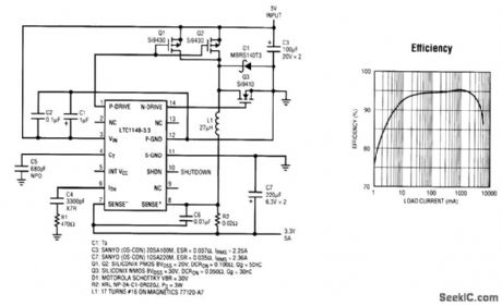
1.8_to_72_MHz_POWER_AMPLIFIER
Published:2009/7/13 2:38:00 Author:May

A novel approach to a 250-W power amplifier (PA) is shown. The driver uses a pair of low-cost ICs, rather than the conventional RF transformer to provide out-of-phase driving signals for the two final MOSFETs. It also provides hard limiting (sine -wave-to-square -wave conversion) of the input signal. The Elantec EL7144C is intended for use as a gate driver. The internal Schmidt trigger allows it to serve as a hard limiter, and the presence of both inverting and noninverting inputs allows a pair to serve as a phase splitter. The RF input is ac-coupled to the noninverting input of U1 and the inverting input of U2. Adjustment of the biases via R6 and R8 allows the transition points to be selected to produce the desired duty ratio (50:50). The phase error between the two EL7144s is about 0.5 ns. (If an oscilloscope is not available, use a voltmeter with a 1-kΩ series resistor and setthe average output voltage to 6 V.) The EL7144s have high input impedances, so R5 provides a 50-V input impedance for the signal source. Input signals in the range of 10 to 100 mW are satisfactory, allowing this PA to be driven directly from a laboratory signal generator or oscillator with buffer.The best switching speed is obtained with VDD1=12 V. Output transistors are ARF440 and ARF441.See parts list. (View)
View full Circuit Diagram | Comments | Reading(1743)
VARIABLE_FREQUENCY_AND_VARIABLE_DUTY_CYCLE
Published:2009/7/16 4:48:00 Author:Jessie
Frequency and duty ratio can be varied independently to generate desired rectangular wave. Uit is used in conventional sawtooth generator. Two transistors provide positive going output when uit emitter voltage exceeds npn emitter voltage. Frequency range is 60 to 1,000 cps.- Transistor Manual, Seventh Edition, General Electric Co. 1964, p 344. (View)
View full Circuit Diagram | Comments | Reading(1131)
95_PERCENT_EFFICIENT_5_V_INPUT_33_V_OUTPUT_DC_TO_DC_CONVERTER
Published:2009/7/13 2:36:00 Author:May
Computing equipment increasingly requires both 3.3-V and 5-V logic supplies, with only the 5-V being readily available. As 3.3-V current demands increase to include microprocessors, coprocessors, DSP processors, and memory, the total power demands on the 3.3-V supply rule out the rela-tively low efficiency and high dissipation of a linear regulator. The circuit shown here supplies 5 A at 3.3 V with over 94-percent efficiency by using the LTC1148-3.3 synchronous switching regulator.This surface-mount solution (L1 is through-hole) requires no heatsinks and very little board space.High efficiency is also maintained at low output currents by implementing Burst mode operation, making the LTC1148-3.3 solution ideal for supplies using normal/sleep modes, such as those in Green PCs. The LTC1148-3.3 can be placed in a shutdown mode, reducing supply current to a mere 22μA. (View)
View full Circuit Diagram | Comments | Reading(534)
ALL_BAND_PREAMP_WITH_WHIP
Published:2009/7/16 4:48:00 Author:Jessie
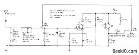

Combination of two-stage preamp and 47-inch telescoping antenna gives overall gain of over 30 dB from 160 to 10 meters, for use with communication and SWL receivers when frequent travel precludes erection of fixed antennas. Use type F, BNC, or SO-239 antenna connector. Tuning coil has 20 taps on 150 turns of No. 28 enamel wire wound on 1/2-inch dowel, with taps at 3, 7, 12, 18, and 25 turns and then about every 10 or 11 turns. Keep leads of at shorted during handling and soldering, to avoid damage by static charges.-K. T. Thurber, Jr., Build A Vacation Special, 73 Magazine, Aug. 1977, p 62-63.
(View)
View full Circuit Diagram | Comments | Reading(893)
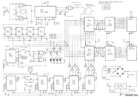
DIGITAL_STOPWATCH
Published:2009/7/13 2:35:00 Author:May
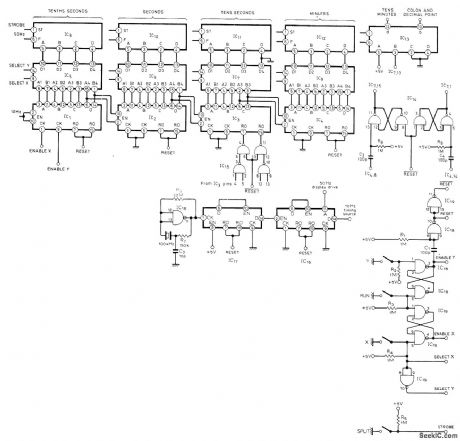
Provides 41/2-digit liquid crystal display for up to 19 min 59.9 s, after which tens of minutes stays at 1 and unit digit recycles from 0 to 9, Gives over 600 hours continuous operation from 5-V mercury battery. Accuracy is determined by 100-kHz crystal oscillator, output of which is divided in two dual decade counters to provide 50-Hz display drive and 10-Hz timing signal. ICs 1, 2, 3, 4, 16, and 17 ai'e CD4518; 5-8 are CD4019; 9-13 are CD4056; 18and 19 are CD4011. Article gives construction and operation details.-P. A. Bimie, Digital EventTimer, Wireless World, Part 1-Dec. 1976, p 32-34 (Part 2-Jan. 1977, p 65-68). (View)
View full Circuit Diagram | Comments | Reading(2191)
THREE_STEP_SEQUENCE_TIMER
Published:2009/7/13 2:34:00 Author:May

Provides three different outputs at predetermined time intervals for initializing conditions during startup or for activating test signals in sequence. Uses three Texas Instruments SN52555 or SN72555 timers which are interchangeable with other 555 timers. Values of R and C at output of each timer determine delays (T=1.1RC). With values shown below timers, output A is 5 V for interval of 1.1 s after switch is closed. At end of this interval, output B goes to 5 V for 0.5 s, after which output C goes to 5 V for 1.5 s to complete sequence. Supply can be 5-15 V.- The Linear and Interface Circuits Data Book for Design Engineers, Texas Instruments, Dallas, TX, 1973, p 7-53-7-61. (View)
View full Circuit Diagram | Comments | Reading(1324)
THREE_TONE_VEHICLE_BEACON
Published:2009/7/16 4:46:00 Author:Jessie


Multitone oscillator modulates 456-kc carrier with three different audio tones whose frequencies are determined by plug-in L-C tanks used in parallel with unstabilized BaTi Transfilter r-f lank circuit.-R. Stapelfeldt, Multitone Oscillcators-New Source of Simultaneous Frequencies, Electronics, 36:1, p 86-87. (View)
View full Circuit Diagram | Comments | Reading(654)
6_TO_25_V_INPUT_5_V_125_A_DC_TO_DC_CONVERTER
Published:2009/7/13 2:33:00 Author:May

One of the keys to success for many portable devices is small size. In many cases, the requirement for a wide battery supply voltage range and high-current, regulated 5-V output seems incompatible with the size requirement. The 500-kHz LT1376, shown in this circuit, provides a powerful, compact power supply. Operating at such a high frequency permits the use of a very small 5-μH surface-mount inductor and a surface-mount output capacitor. In addition, the intemal switch has just 0.4 Ω of ON resistance, which reduces power loss and boosts efficiency to 88 percent. A special boost pin and circuitry reduces the minimum operating supply voltage in step-down applications. The maximum current rating of the switch is 1.5 A. The input voltage range extends from 6 to 25 V and is well matched for many battery-pack assemblies. The typical supply current is 4 mA, whereas the shutdown current is just 20 μA. (View)
View full Circuit Diagram | Comments | Reading(780)
Tone circuit diagram made by LM1036
Published:2011/7/15 10:58:00 Author:Nancy | Keyword: Tone
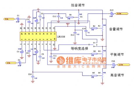
LM1036 is a voltage controlled double channel, tone (high/low), volume, left and right volume adjustment IC. It has a loudness switch to compensate the ear characteristic curve when the volume is small. Because it is controlled and adjusted by the voltage, it can use the single-chip microcomputer control circuit to adjust tone, volume, balance and equal loudness, and can not use the offensive duplex (or single) potentiometer completely, and this can't effect the tone quality even using it. (View)
View full Circuit Diagram | Comments | Reading(4189)
ELECTROSCOPE_CIRCUIT
Published:2009/7/16 4:46:00 Author:Jessie
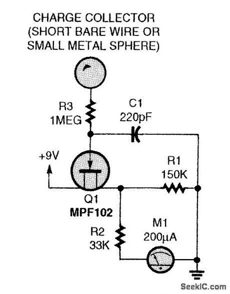


This circuit detects a charged object at a respectable distance and displays the polarity (positive, negative, or earth-grounded) and relative intensity. In operation, C1 reduces ac noise but lowers the sensitivity a bit. The MPF102 and R1 form a voltage divider. When the FET's gate is earth-grounded, the divider's output will be about 4.5V, giving a half-scale reading on M1, a 200-μA meter. A positively charged object (like cotton-rubbed glass) will give a positive deflection from half scale, and a negatively charged object (a plastic comb, for example) will give a negative meter deflection. The whole circuit (including the 9-V supply) should be in a metal enclosure. (View)
View full Circuit Diagram | Comments | Reading(1086)
ROCKET_ROLL_CONTROL
Published:2009/7/13 2:31:00 Author:May
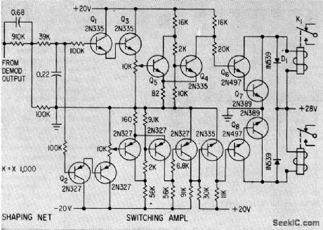
Signal from rollchannel demodulator is shaped for two-section switching amplifier that energizes roll jet relays.-R. E. King and H. Low, Solid-State Guidance For Able-Series Rockets, Electronics, 33:5, p60-63. (View)
View full Circuit Diagram | Comments | Reading(755)
POS CDMA/TDMA PA driver amplifier FR2324 pin data
Published:2011/8/4 2:46:00 Author:May | Keyword: driver amplifier

RF2324 is CDMA/TDMAPA driver amplifier with very large dynamic range. It is designedfor 1800MHz emission digital PCS signal.The device is used as aPA driver amplifier with outstanding properties, it can solve the low emission noise power problem which is cared by digital user. RF2324 has the property of power down control ,and itcan total close the device. RF2324 adopts standard small 8 pins MSOP plastic package. Its pin array is shown in the diagram.
The pin function is shown in the follwing diagram
(View)
View full Circuit Diagram | Comments | Reading(667)
9_V_INPUT±5_V_OUTPUT_DC_TO_DC_CONVERTER
Published:2009/7/13 2:31:00 Author:May
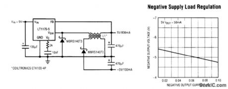
Many dc-to-dc converter applications require regulated complementary output voltages from a single loosely regulated source. A common use for this is supplying 5 V and -5V to a video op amp for amplification or cable driving. Accomplishing this task in a space-effective manner with a minimum of corrtponents is a challenge for a designer. The LT1176-5 circuit shown here uses a single integrated switching regulator and an off-the-shelf inductor with an extra winding to generate ±5 V from an 8- to 12-V input. The circuit is designed to supply 5 V as the main output with up to 800 mA of load current, and -5 V as a secondary output with up to 100 mA load current. Regulation is adequate for most opamp circuits: 5-V regulation will be ±3 percent and -5-V regulation is about ±10 percent for loads between -10 and -100 mA. The LT1176-5 providesacomplete 100-kHz switching regulator with a 1.2-A on-chip switch in a thin 20-lead SO package. The enhanced thermal characteristics of the fused-lead SO package allow higher power outputs than were previously possible with SOs. (View)
View full Circuit Diagram | Comments | Reading(714)
OP_AMP_RESPONSE_NULL_CIRCUIT
Published:2009/7/13 2:28:00 Author:May
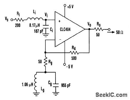
A sharp null can be achieved in a current feedback op amp's frequency response by adding a sharp cutoff filter. The response is modified by adding a resonant circuit in series with the gain-setting resistor Rg. (View)
View full Circuit Diagram | Comments | Reading(604)
STEREO_AUDIO_COMPRESSOR
Published:2009/7/13 2:28:00 Author:May
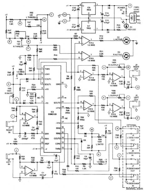

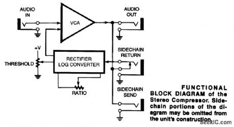
The block diagram of the stereo compressor is shown. The input signal is fed to a voltage-con-trolled amplifier (VCA) that has a nominal gain of unity. Some of the output signal is fed to a precision rectifier followed by a logarithmic converter circuit. The output of this block is a dc voltage proportional to the log of the average level of the input signal. By sending some of this dc control voltage to the VCA, the gain of the VCA is automatically reduced when the input signal exceeds a user-determined threshold level. It is important to note that the signal level is determined after the VCA and not before. This allows the output level to increase and sound normal, but not increase as much as the input signal does. By varying the amount of feedback, the compression ratio is adjusted, which, in conjunction with the THRESHOLD control, determines the operating characteristics of the compressor. The optional sidechain jacks permit external processing of the audio signal or substitution of a completely different audio signal as the control signal. This add-on circuitry lets the user ex-periment and achieve some useful audio effects. (View)
View full Circuit Diagram | Comments | Reading(2737)
TIMER_WITH_MEMORY
Published:2009/7/13 2:27:00 Author:May
Time elapsed since initial triggering at start of event is shown on 2digit MAN-1 display in seconds or tenths of seconds and written into memory, Up to 16 event times can be stored for later readout. Free-running mode counts off seconds or tenths of seconds on display. Article covers construction and operation. Circuit was Science Fairwinner. Gate and opamp types are not critical.-M. Event Timer with Memory.73 Magazine, 1977,p 72-74. (View)
View full Circuit Diagram | Comments | Reading(926)
70_V_INPUT_5_V_700_mA_TELECOM_CONVERTER
Published:2009/7/13 2:27:00 Author:May

Telecom dc-to-dc conversion applications are usually complex because of the wide input voltage range of -30 to -70 V. Either big, expensive converter modules or space- and component-intensive discrete solutions are normally required to handle these higher voltages. The LT1082 contains a 1-A switch that can handle 100 V, enabling a -48-V-to-5-V converter to be designed with minimal size and cost. Features include foldback of the 60-kHz switching frequency under short-circuit condi-tions, protecting the LT1082 and power components from excessive power dissipation. The LT1082 dc-to-dc converter circuit provides up to 750 mA of output current, and the solution costs less than a modular supply of similar capabilities. (View)
View full Circuit Diagram | Comments | Reading(751)
PROXIMITY_CONTROL
Published:2009/7/13 2:27:00 Author:May
Gain of Hartley oscillator is set so oscillation is maintained only when Q of resonant circuit is normal. When ferrous or nonferrous materials come near pickup coil, Q is reduced, oscillation stops, and output tube conducts, to pull in relay for counting or for controlling industrial machinery. Can be set for operating range of from 1/8th inch to 1 foot.-D. Elam, Proximity Transducer Uses Rapid Relay, Electronics, 31:25, p73. (View)
View full Circuit Diagram | Comments | Reading(566)
200_W_AT_25_kHz
Published:2009/7/13 2:26:00 Author:May

Two Deleo DTS-403 highvoltage silicon transistors are connected as push-pull oscillator operating on 150-VDC bias.Efficiency is 78% at full load. Diodes serve alternately as steering and clamp diodes.- 25 kHz High Efficiency 200 Watt Inverter, Deleo, Kokomo, IN, 1971, Application Note 47. (View)
View full Circuit Diagram | Comments | Reading(2845)
| Pages:723/2234 At 20721722723724725726727728729730731732733734735736737738739740Under 20 |
Circuit Categories
power supply circuit
Amplifier Circuit
Basic Circuit
LED and Light Circuit
Sensor Circuit
Signal Processing
Electrical Equipment Circuit
Control Circuit
Remote Control Circuit
A/D-D/A Converter Circuit
Audio Circuit
Measuring and Test Circuit
Communication Circuit
Computer-Related Circuit
555 Circuit
Automotive Circuit
Repairing Circuit