
Circuit Diagram
Index 727
0_to_±35_V
Published:2009/7/16 20:49:00 Author:Jessie
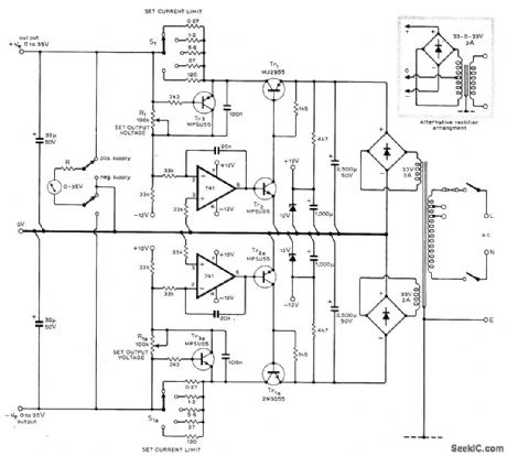
Twin stabilized DC supply uses ganged pots R1and R1a to set both positive and negative regulated outputs at any desired value up to 35 V. Input supplies from bridge rectifiers also provide ±12 V lines for 741 opamps. Load regulation is within 2 mV from no load to full 2-A maximum output. Output hum, noise, and ripple are together only 150 μV and independent of load.-J. L. Linsley Hood, Twin Voltage Stabilized Power Supply, Wireless world. Jan.1975, p 43-45.
(View)
View full Circuit Diagram | Comments | Reading(1752)
VARIABLE_PULSER
Published:2009/7/16 20:49:00 Author:Jessie
Operates with any power supply voltage from l.5 to 20 v, und generates symmetrical or nonsymmetrical low. impedance pulses from 0.5 ppm to above 200,000 pps. Used for controlling repetitive operation of certain analog computers, and as source for checkout of digital circuits. -J. V. Gaudiosi, Variable Pulse Generator, EEE, 11:2, p 27-28. (View)
View full Circuit Diagram | Comments | Reading(729)
FET_TESTER
Published:2009/7/16 20:49:00 Author:Jessie
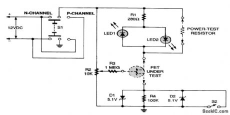
In operation, either a P-channel or an N-channel FET can be plugged in and tested by selecting the proper polarity with the power switch. With the control potentiometer (R2) at ground potential, the FET under test will conduct until the pinchoff voltage is reached. The LED will not turn on at this point because of the low current. This pinchoff voltage can be read at the top of resistor R4 with a high-impedance voltmeter. Increasing the potentiometer will decrease the pinchoff voltage until the FET conducts and an LED turns on. The LEDs give a rough indication of conduction. A more accurate reading is obtained by monitoring the voltage drop across the drain resistor. For a quick go/no-go FET check, the switch (S2) across the zeners can be closed. The associated LED should light and should go out when the switch is opened. If it does not, the FET is bad or is connected wrong, or the selector switch is set for the wrong-polarity FET. The 1-MΩ resistor (R3) at the gate connection is protection for the potentiometer should a unit under test short, it provides current limiting for the protection diodes in the gate of the CMOS FETs. (View)
View full Circuit Diagram | Comments | Reading(0)
WIDEBAND_CURRENT_FEEDBACK_AMPLIFIER
Published:2009/7/13 1:45:00 Author:May

When using multipliers such as the LM1496 or MC1496, low-value output resistors are necessary to obtain maximum bandwidth. This reduces the output swing available, which necessitates a differ-ential high-gain, wideband amplifier. The amplifier has a differential gain (AV,diff) of 50 and a band-width of about 50 MHz, giving it a total gain-bandwidth product of 2.5 GHz. It also provides an output swing of 18 V p-p from a 112-V supply. Transistors Q1 and Q2 form a differential pair that drives Q3 and Q4. Feedback is provided to the emitters of Q1 and Q2 by R6, C1 and R7, C2, which bootstraps the input impedance and sets the overall gain. Q5 and Q6 provide about 15 mA of current each, pro-viding most of the sourcing current for the load. The basic design equations are provided to modify component values to suit different applications.Simply envision the circuit is as a differential current-feedback amplifier, with the low-imped-ance port being the emitters of Q1 and Q2, and the current output as the collectors of Q3 and Q4.Because the output is a bridge circuit and the maximum positive current is set by R6, R7 and Q5, Q6, the output is short-circuit-protected between resistors R8 and R9. RI can be replaced by a current source to reduce the common-mode gain. The main criterion is to balance the currents at the emit-ters of Q1 and Q2 to give a common-mode output voltage of VCC/2. Some care should be taken when driving capacitive load because the circuit can oscillate under such conditions. (View)
View full Circuit Diagram | Comments | Reading(1929)
STEP_DOWN_REGULATOR
Published:2009/7/16 20:48:00 Author:Jessie

There are several versions of the LM2575T. The device used here has an ADJ suffix, which indicates that it has an adjustable output voltage. Pin 4 connects to the inverting input of the internal error amplifier. This amplifier's noninverting input is fed from a 1.2-V reference source. A discrete potentiometer connected across the output and feeding into pin 4 enabling the output voltage to be set at any figure above 1.2 V. In this case, the potentiometer is formed by VR1 in series with resistor R1. The adjustment range provided by VR1 is from 1.2 V to a little over 16 V. Higher output voltages can be accommodated by making R1 lower in value, but a circuit of this type is mainly used where there is a large voltage difference between the input and the output. Consequently, it is unlikely to be used with output voltages of more than about 16 V. The absolute maximum input voltage is 40 V. (View)
View full Circuit Diagram | Comments | Reading(2369)
GATED_ASTABLE_PULSE_TRAIN_GENERATOR
Published:2009/7/16 20:47:00 Author:Jessie
Uses standard logic circuits with self-completing action to produce pulse train having any desired integral number of pulses. First pulse starts when S1 is closed, and last pulse is completed when S1 is open. Selfcompleting action is produced by or function of S1 und CR1.-M. Neidich, Self-Completing Gated Astable, EEE, 13:1, p 66 and 75. (View)
View full Circuit Diagram | Comments | Reading(1009)
NE602_DC_SUPPLY_INTERFACE
Published:2009/7/16 20:47:00 Author:Jessie
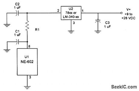
This is one method of deriving the 4.5-to 8.0-Vdc supply needed by the NE602 chip. (View)
View full Circuit Diagram | Comments | Reading(728)
SIMPLE_TRANSISTOR_CHECKER
Published:2009/7/16 20:47:00 Author:Jessie
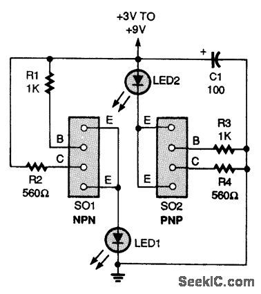
When a T092-type transistor is placed in the correct socket, if the transistor is good, the circuit turns on, according to the kind of transistor being tested. For example, if a good NPN unit is tested, LED1 turns on. Note that two emitter positions are in each socket. Transistors have different pin configurations. Some are BBC, and some are ECB. If you don't know the configuration, you can test all the possible pin positions until an LED turns on. You'll need to know if the transistor is an NPN or a PNP type, however. The supply voltage can be 3 to 9 V. There is no power switch because, without a socketed transistor, capacitor C1 is the only load on the battery. For the sockets, use an eight-pin, mini-DIP socket. (View)
View full Circuit Diagram | Comments | Reading(1418)
STEP_UP_REGULATOR
Published:2009/7/16 20:46:00 Author:Jessie
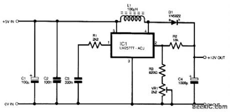
Refer to the figure for the circuit diagram of the step-up regulator. This circuit is based on an LM2577T-ADJ, which is designed to give a combination of high performance and simplicity. It can provide output currents of up to 3 A, and it has both overcurrent and thermal-protection circuits built in. It requires a minimum input potential of 3.5 V, and it shuts down automatically if the input voltage is inadequate. The maximum input voltage is 40 V. Capacitors C1 and C2 provide supply decoupling at the input, and C3 and resistor R1 provide frequency compensation. Inductor L1, diode D1, and an internal switching transistor of IC1 form a standard step-up output stage, with output smoothing provided by capacitor C4. Resistors R2 and R3 and preset VR1 form a potential divider that controls the output voltage. IC1 has an internal 1.2-V reference generator, and the voltage at pin 2 is, therefore, stabilized at this figure. With the specified values in the potential divider circuit, the output voltage range is around 9.5 to 25 V. (View)
View full Circuit Diagram | Comments | Reading(2236)
TRANSISTOR_BETA_DISPLAY
Published:2009/7/16 20:45:00 Author:Jessie


Falloff in beta with increasing collector current is displayed on auxiliary cro over range of 0 to 200 ma, for constant collector voltages up to 8 v.-R.Zuleeg and J. Lindmayer, Sweep Equipment Displays Transistor Beta, Electroics,31:49, p 100-101. (View)
View full Circuit Diagram | Comments | Reading(1029)
BASIC_BOOST_CONVERTER_CIRCUIT
Published:2009/7/13 1:43:00 Author:May
This boost converter with a single switching transistor depends on the transformer for energy storage. (View)
View full Circuit Diagram | Comments | Reading(943)
BASIC_BUCK_CONVERTER_CIRCUIT
Published:2009/7/16 20:45:00 Author:Jessie

The buck regulator is an alternative single-transistor converter. Series transistor Q1 chops the input voltage and applies the pulse to an averaging inductive-capacitive filter, consisting of L1 and C1.The output voltage of this simple filter is lower than its input voltage. (View)
View full Circuit Diagram | Comments | Reading(938)
500_kHz_33_V_TO_12_V_DC_CONVERTER
Published:2009/7/13 1:43:00 Author:May

The LT1309 500-kHz micropower dc-to-dc converter circuit shown provides a compact 12-V supply. High-frequency operation permits the use of low-inductance and low-capacitance values for surface-mount parts. The LT1309 provides 60 mA of output current at 12 V, required for 8-bit-wide flash memory chips. In addition, when the flash memory card is removed, the LT1309 can be shut down by the system, reducing current draw to 6 μA. A soft-start feature allows the output voltage to ramp up to 12 V over a period of time, minimizing inrush current needed from the 3.3-V supply to charge the PCMCIA input capacitance. An active-low VPP VALID output signals the system that the 12-V supply is within regulation after being switched on. (View)
View full Circuit Diagram | Comments | Reading(871)
ORYSTAL_RADIO_AMPLIFIER
Published:2009/7/13 1:43:00 Author:May

If you'd like to hear your crystal set at a comfortable, room-filling volume, hook it up to this amplifier. (View)
View full Circuit Diagram | Comments | Reading(937)
±20_V_CHARGE_PUMP_BOOST_CONVERTER
Published:2009/7/13 1:41:00 Author:May

A low-power converter of 5 to ±20 V can be made surprisingly small by enhancing a dual-output charge-pump IC with an extra boost stage composed of discrete diodes. Such supplies are useful for LCD power supplies, LCD bias, and varactor tuners. The MAX864 on its own can generate ±10 V (minus load-proportional losses) from a 5-V input, or ±6.6 V from a 3.3-V input. Using additional diode-capacitor stages, these outputs can be doubled again to approximately ±4Vin or multiplied by 1.5 to approximately ±3Vin. Note that the external diode/capacitor network connects to C1 for ±15-V outputs or to C2 for ±20V outputs. (View)
View full Circuit Diagram | Comments | Reading(1174)
LED_TEST_CIRCUIT
Published:2009/7/16 20:45:00 Author:Jessie


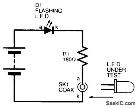
The circuit is intended as a simple one to enable spot testing of bulk surplus LEDs. A flashing LED is used (D1) with a 9-V battery, and is connected to a coaxial socket. When a test LED is placed across the socket (anode to the inner conductor), both the flashing LED and the test LED will flash. No on-off switch is necessary (View)
View full Circuit Diagram | Comments | Reading(1332)
ELECTRET_MIKE_PREAMP_WITH_PTT_CIRCUIT
Published:2009/7/13 1:41:00 Author:May

The schematic of electret mike element and amplifier circuit All resistors are 1/4-W units. The mike connector is an RS 274-284. (View)
View full Circuit Diagram | Comments | Reading(1911)
PUSH_PULL_AUDIO_LINE_DRIVER
Published:2009/7/13 1:39:00 Author:May

A line driver for 600 Ω can be configured from two IC op amps. U1A and U1B are Analog Devices OP-275. These devices feature low power consurrtption, low THD, and high slew rate. (View)
View full Circuit Diagram | Comments | Reading(1544)
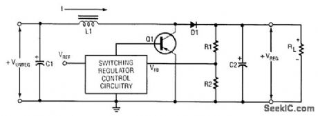
NEGATIVE_BUCK_REGULATOR
Published:2009/7/16 20:44:00 Author:Jessie

This circuit adopts a step-up (boost) dc-to-dc controller for use in a negative buck-regulator application. The supply voltage must be negative, and it must deliver 160 to 750 mA. Although the boost-regulator IC operates in a buck-regulator circuit, its standard connections enable proper control of Q1. The output voltage, however, must be inverted by an op amp for proper voltage feedback: The load is referred to the most positive supply rail instead of to 101's ground terminal, so the controller must increase its duty cycle as Vout (referred to that terminal) increases. The op amp there-fore inverts the feedback Signal and shifts it to match the 1.5-V threshold internal to IC1. IC1 is configured in its nonbootstrapped mode, which provides an adequate gate-drive signal (ground to -5.2 V) for the external MOSFET (Q1). With Vout set to -3 V and the output current ranging from 160 mA to above 700 mA, the circuit's conversion efficiency ranges from 84 percent to as high as 87.5 percent. (View)
View full Circuit Diagram | Comments | Reading(1459)
MULTIPURPOSE_MINIAMPLIFIER
Published:2009/7/13 1:38:00 Author:May
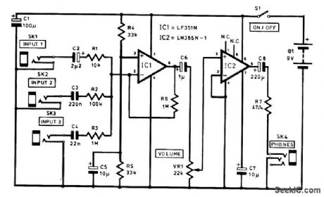
This circuit uses two audio IC amplifiers, one for a preamp and one for a power output stage. Three audio inputs are provided-low (1 mV), medium (10 mV), and high (100 mV) input-to drive a pair of headphones or a strtall speaker. The LM386 is good for 0.5 W or more output, and a small speaker can be connected directly to the junction of C8 and R7. A series combination of a 22-Ω resistor and a 0.1-mF capacitor should be connected between this point and ground to suppress possible high-frequency oscillations in this case. (View)
View full Circuit Diagram | Comments | Reading(1360)
| Pages:727/2234 At 20721722723724725726727728729730731732733734735736737738739740Under 20 |
Circuit Categories
power supply circuit
Amplifier Circuit
Basic Circuit
LED and Light Circuit
Sensor Circuit
Signal Processing
Electrical Equipment Circuit
Control Circuit
Remote Control Circuit
A/D-D/A Converter Circuit
Audio Circuit
Measuring and Test Circuit
Communication Circuit
Computer-Related Circuit
555 Circuit
Automotive Circuit
Repairing Circuit