
Circuit Diagram
Index 726
TWO_CELL_5_V_500_mA_CONVERTER
Published:2009/7/13 1:55:00 Author:May

Hand-held instruments, PCMCIA cards, and portable communications gear often require high current for their operation, although only for short periods at a time. Current of 500 mA at 5 V can be obtained from a two-cell battery using a switching regulator controller IC, an external switch transistor, and some discrete components, but the solution is inefficient, space-intensive, and cumbersome. The LT1302 was designed to provide higher output currents by using an integrated 2-A low-loss switch. An output current of 500 mA at 5 V with 85 percent efficiency is possible from two AA cells. Component size is minimized by using a fixed-frequency 220-kHz PWM architecture. The circuit maintains high efficiencies at low load currents by automatically switching to Burst mode operation at lower switch currents. (View)
View full Circuit Diagram | Comments | Reading(1059)
The high-voltage circuit diagram of DC rectifier tube filament center-tap
Published:2011/8/4 1:27:00 Author:Ecco | Keyword: high-voltage , DC rectifier tube , filament center-tap

View full Circuit Diagram | Comments | Reading(984)
ACCURATE_LOG_AMPLIFIER
Published:2009/7/13 1:54:00 Author:May

The log circuit consists of an instrumentation amp and an Op amp together with a diode-connectedtransistor that produces a voltage proportional to the logarithm of the current A circuit consisting of avoltage reference, an instrumentation amp,and an op amp,togetherwith a diode-connected transistor,acts as a reference circuit. A thermometer IC,a fixed-gain instrumentation amp,and a divider circuitprovide the necessary temperature compensation and scaling for a transfer function∶Vout51.985 log10 (Vin/1V)Vref must be set to 1.000 V and, with Vin 5Vref, the gain adjust has to be set so that VO 50 V. Calirelbration low input voltage is done by changing buffer A4's offset voltage. (View)
View full Circuit Diagram | Comments | Reading(2281)
Adjustable regulated power supply circuit with overload and short circuit protection function
Published:2011/7/19 9:46:00 Author:Nancy | Keyword: Adjustable regulated power supply, overload, short circuit protection
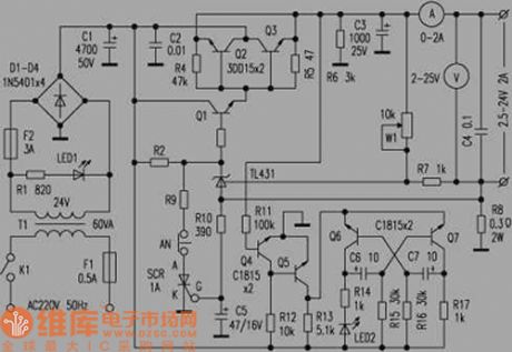
The circuit has the overload, short circuit protection and alarm function. Under the overload condition, the voltage drop of the resistor R8 increases. When the voltage drop reaches 0.6V, SCR conducts, which makes the Q1 base electric potential drop to about 1V, so the transistor Q1 and the regulating transistor Q2, Q3 cut off to protect regulating transistor from burning out. After Q2 and Q3 cut off, the output voltage is zero and the electronic switch Q4 cut off, Q5 conducts, which make the multivibrator composed by Q6 and Q7 start oscillation (dozens of Hertz), light-emitting diode LED2 flashes to alarm. (View)
View full Circuit Diagram | Comments | Reading(2086)
Array speech synthesis series circuit diagram
Published:2011/8/4 1:25:00 Author:Ecco | Keyword: Array speech synthesis

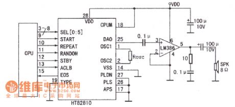
The speech synthesis circuit uses four series more input or output components to form the matrix keyboard. Figure shows HT83XXX series of 32-key application circuit diagram. This series of voice circuits can achieve statement spelling and other functions by plugging the microprocessor (CPU).
This is the connection diagrambetween the CPU and HT82810.
(View)
View full Circuit Diagram | Comments | Reading(1360)
SHUTDOWN_PROTECTION
Published:2009/7/13 1:52:00 Author:May

Used with digital logic to prevent generation of false logic signals when power supply is turned on or turned off, FETs sense +15 V and -15 V supplies and conduct when either supply drops below pinchoff voltage, activating shutdown output. With values shown, shutdown output is disabled when supplies exceed about 4 V, to provide normal operation.-E. Burwen, Power-Supply Monitor Suppresses False Output Signals, EDN Magazine, Nov. 5, 1977, p 110 and 112. (View)
View full Circuit Diagram | Comments | Reading(732)
INDUCTORLESS_-5_V_CONVERTER
Published:2009/7/13 1:51:00 Author:May
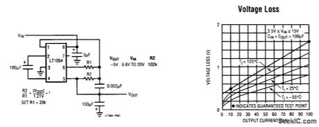
Switched capacitor voltage converters are great for supplying an unregulated negative voltage from a positive supply. To provide a regulated negative voltage, a linear regulator is normally required.The LT1054 eliminates the extra voltage regulator by adding a pair of feedback resistors, as shown here. An internal feedback circuit allows full regulation of the output voltage with changes in input voltage and load cutpent. With a minimum input of 6.5 V, the LT1054 can produce a regulated -5-V output at loads of up to 100 mA max. External components required include four capacitors and two resistors. (View)
View full Circuit Diagram | Comments | Reading(951)
MICROPOWER_POSITIVE_TO_NEGATIVE_CONVERTER
Published:2009/7/13 1:49:00 Author:May

Switched capacitor voltage converters are a convenient way to generate a local negative supply for biasing special circuitry, but have been limited by CMOS processes to 10 V of supply or less. The LTC1144 voltage converter overcomes this limitation, extending the maximum input voltage to 20 V. Still, the part retains the low power of CMOS operation. The LTC1144 circuit shown here generates a negative supply voltage of -13.8 V typ. (-12.6 Vmin) from a 15-V input at a maximum load current of 20 mA. Higher load currents are possible at slightly lower output voltages. The low-cost circuit includes two surface-mount capacitors, minimizing board space. A supply current of 1.2 mA (max.) results in high conversion efficiency, while just 8 μA of supply current is consumed in shutdown, making the LTC1144 excellent for use in battery-powered systems. (View)
View full Circuit Diagram | Comments | Reading(1217)
FAlL_SAFE_LIGHT_TIMEB
Published:2009/7/13 1:49:00 Author:May

National MM5309 clock IC is used as timer in circuit that maintains timing with adequate accuracy during periods of power-line failure and retums automatically to 60-Hz line as soon as power is restored. Applications include control of lights in unoccupied home. Timing action tums on lights for 4h period every 24 h. When power is applied, intemal multiplex circuit strobes each digit until digit with connected diode is accessed. This digit stops multiplex scanning, and BCD outputs present data from selected digit as control waveform whose edges determine timer data.- MOS/LSI Databook, National Semiconductor, Santa Clara, CA, 1977, p 1.74-1-77. (View)
View full Circuit Diagram | Comments | Reading(760)
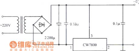
Integrated regulated voltage supply basic circuit with fixed output
Published:2011/7/19 9:25:00 Author:Nancy | Keyword: fixed output, integrated regulated voltage supply
View full Circuit Diagram | Comments | Reading(536)
500_W_AT_20_kHz
Published:2009/7/13 1:49:00 Author:May
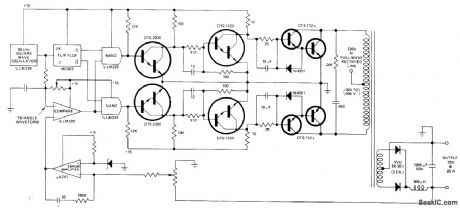
Uses four Delco DTS-712 transistors in push-pull Darlington configuration, with pulse-width modulation on push-pull inverter providing regulation. Can be operated from 220-VAC three-phase full-wave rectified line. Efficiency is up to 80%. Square-wave output of 40-kHz primary oscillator drives JK flipflop that generates complementary square waves and divides frequency by 2 with necessary symmetry. NAND gates establish primary ON/OFF periods of power stage. Portion of output signal is compared to reference voltage, and error signal is fed to NAND gates to give regulation better than 0.1% for load range of 200-500 W or line range of 300-400 V.- A 20 kHz, 500 W Regulating Converter Using DTS-712 Transistors, Delco, Kokomo, IN, 1974, Application Note 55. (View)
View full Circuit Diagram | Comments | Reading(1796)
monitoring negative power supply circuit
Published:2011/7/19 10:05:00 Author:Nancy | Keyword: negative power supply
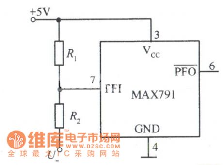
View full Circuit Diagram | Comments | Reading(553)
MICROPOWER_STET_UP_CONVERTER
Published:2009/7/13 1:48:00 Author:May

This circuit can start with inputs as low as a diode drop, i.e., 0.6 V. It provides a 5-V output with 15-mA current capability, but for this application, the load current must be limited. The circuit pow-ers a meter from the drop across a single diode in a 4- to 20-mA current loop, and provides 77 percent efficiency at a current of 0.5 mA (with diode D6 shorted). Load current available to the meter (Iload) is limited by the 4-mA minimum loop current. Transistor Q1 and transformer T1 form a resonant tank circuit that self-oscillates at a frequency of approximately 1/L1R1.R1 is a current-limiting resistor. At 50 kHz, with an input of 0.6 V, the value shown for resistor R1 (33 Ω) limits the maximum current into the base of transistor Q1 to 20 mA. The primary inductance of transformer T1, although not a crucial parameter, should be 660 μH for this value resistor of R1.
(View)
View full Circuit Diagram | Comments | Reading(976)
HT16500 audio integrated chip circuit diagram
Published:2011/8/4 1:39:00 Author:Ecco | Keyword: audio integrated chip


Theplastic DIP pin diagram and the typical application circuit of HT16500audio integrated circuit are as below:
(View)
View full Circuit Diagram | Comments | Reading(580)
SATURATING_MVBR_ON_OFF_CONTROL
Published:2009/7/13 1:47:00 Author:May

Used with relays and other electromechanical devices where current ratio must be 10 between on and off conditions. Operation is same as Eccles-Jordan, except that current drive for holding Q2 on is furnished through R2 and R3 rather than through Q1 collector load.Designed for relay that is energized by 8ma and drops out at 0.5 ma, Trigger input should be between 14 and 20V, with rise time of 10 microsec. Input circuit needs 5 millisec to recover from positive signal before next trigger is applied. 2N333 has been dropped from Preferred List, but 2N335 can be used if operating point is adjusted for its higher beta.-NBS, Handbook Preferred Circuits Navy Aeronautical Electronic Equipment, Vol, II, Semiconductor Device Circuits, PSC 17 (originally PC 251), p17-2. (View)
View full Circuit Diagram | Comments | Reading(647)
UJT_SCR_TIMER
Published:2009/7/13 1:47:00 Author:May

Use of large capacitance for C1 in simple UJT relaxation oscillator providestime delay action for triggering SCR controllingrelay R1 provides convenient adjustment ofdelay SCR can be 6-A 50-V Radio Shack 2761089. Relay is 275-004,-F.M.Mims, Semiconductor Projects, Vol 2, Radio Shack, Fort Worth,TX,1976,p 50-61. (View)
View full Circuit Diagram | Comments | Reading(2449)
NEGATIVE_SUPPLY_GENERATOR
Published:2009/7/16 20:49:00 Author:Jessie
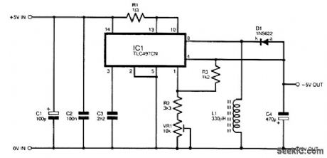
The TLC497CN is very useful for applications that do not involve high output currents. It provides a cost-effective means of providing a negative supply of up to about 150 mA. A circuit diagram for an inverter based on this device is shown. The efficiency of the circuit is typically a little over 50 percent with an input potential of 10 V, but is significantly under 50 percent with an input supply of 5 V. Capacitors C1 and C2 are supply-decoupling components on the input supply. Resistor R1 is the series resistance in the current-limiting circuit at the input to IC1. This is an essential safety feature because the circuit will Often be fed from a high-current supply that could almost instantly fry IC1 in the event of an overload on the device's output. Capacitor C3 is the timing component in the oscillator section of the PWM. The TLC497CN uses a fixed pulse width and a variable clock frequency to control the average output voltage. (View)
View full Circuit Diagram | Comments | Reading(799)
rotary disc switch principle circuit
Published:2011/7/19 10:19:00 Author:Nancy | Keyword: rotary disc switch
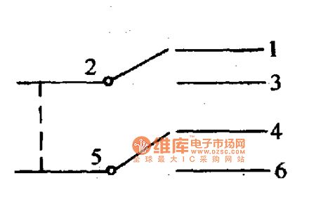
This switch looks very complex, it is actually a double pole double throw switch. The welding piece 2 and 5 are pole , and the other four leading welding pieces are throw (shown as the figure). When the rotary disc turns to + , 2 and 3 conduct, 5 and 6 conduct; When the rotary disc turns to - , 2 and 1 conduct, 5 and 4 conduct. Through the rotary disc has ten teeth, and can turn ten times, but there are only + and - two states mentioned as aobove. (View)
View full Circuit Diagram | Comments | Reading(481)
RASTER_VERTICAL_SWEEP
Published:2009/7/16 20:49:00 Author:Jessie

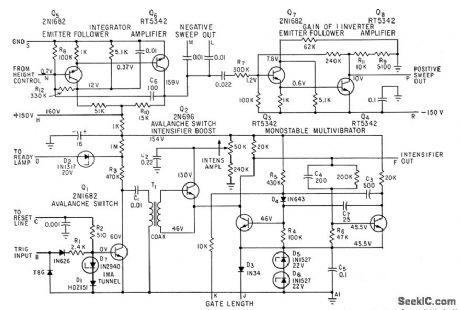
Q1 in shaper triggers intensifier pulse for test oscilloscope using tv type scanning, while remainder of circuit generates vertical sweep for scope used to measure time intervals in range of 0.5 to 100 microsec with time resolution of 0.05 microsec.-R.P.Rufer and W. A. Karlotski, Use Raster Oscilloscopes for Faster time Measurements, Electronics, 35:52, p 38-42. (View)
View full Circuit Diagram | Comments | Reading(1265)
10_s_TO_10_min
Published:2009/7/13 1:46:00 Author:May

Away of ten LEDs serves for measuring time intervals up to 10 min, for timing phone calls, photographic exposures, and cooking. Pulse output rate of UJT oscillator Q1 is determined by value of C1 and setting of R1. Pulses are counted by 7490 which gives total count in binary form. 7490 recycles after each l0 counts. 7441 converts binary signals from 7490 to decimal outputs driving LED indicators. Each LED glows in sequence as count advances from 0 through 9 and repeats. For 10-pin timer, adiust R1 until first LED stays on for exactly 1 min. For 10-stimer, adiust R1 for blink rate of 1 s per LED.-F. M. Mints, Optoelectronic Proiects, Vol, n, Radio Shack, Fort Worth, TX, 1977, 2nd Ed., p 67-78. (View)
View full Circuit Diagram | Comments | Reading(734)
| Pages:726/2234 At 20721722723724725726727728729730731732733734735736737738739740Under 20 |
Circuit Categories
power supply circuit
Amplifier Circuit
Basic Circuit
LED and Light Circuit
Sensor Circuit
Signal Processing
Electrical Equipment Circuit
Control Circuit
Remote Control Circuit
A/D-D/A Converter Circuit
Audio Circuit
Measuring and Test Circuit
Communication Circuit
Computer-Related Circuit
555 Circuit
Automotive Circuit
Repairing Circuit