power supply circuit
NEGATIVE_SUPPLY_GENERATOR
Published:2009/7/16 20:49:00 Author:Jessie | From:SeekIC

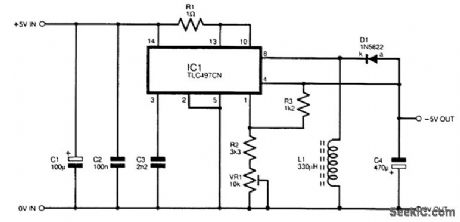
The TLC497CN is very useful for applications that do not involve high output currents. It provides a cost-effective means of providing a negative supply of up to about 150 mA. A circuit diagram for an inverter based on this device is shown. The efficiency of the circuit is typically a little over 50 percent with an input potential of 10 V, but is significantly under 50 percent with an input supply of 5 V. Capacitors C1 and C2 are supply-decoupling components on the input supply. Resistor R1 is the series resistance in the current-limiting circuit at the input to IC1. This is an essential safety feature because the circuit will Often be fed from a high-current supply that could almost instantly fry IC1 in the event of an overload on the device's output. Capacitor C3 is the timing component in the oscillator section of the PWM. The TLC497CN uses a fixed pulse width and a variable clock frequency to control the average output voltage.
Reprinted Url Of This Article:
http://www.seekic.com/circuit_diagram/Power_Supply_Circuit/NEGATIVE_SUPPLY_GENERATOR.html
Print this Page | Comments | Reading(3)

Article Categories
power supply circuit
Amplifier Circuit
Basic Circuit
LED and Light Circuit
Sensor Circuit
Signal Processing
Electrical Equipment Circuit
Control Circuit
Remote Control Circuit
A/D-D/A Converter Circuit
Audio Circuit
Measuring and Test Circuit
Communication Circuit
Computer-Related Circuit
555 Circuit
Automotive Circuit
Repairing Circuit
Code: