
Circuit Diagram
Index 733
Kejian K518 mobile phone component cable distribution diagram
Published:2011/8/3 21:38:00 Author:Ecco | Keyword: Kejian , mobile phone , component cable distribution

View full Circuit Diagram | Comments | Reading(1167)
Inspur CU100 mobilephone cable connection diagram
Published:2011/8/3 21:47:00 Author:Ecco | Keyword: Inspur , mobilephone cable connection

View full Circuit Diagram | Comments | Reading(710)
Inspur CU100 mobile phone cable components distribution diagram
Published:2011/8/3 21:46:00 Author:Ecco | Keyword: Inspur, mobile phone , cable components distribution

View full Circuit Diagram | Comments | Reading(738)
Vacuum tube headphone amplifier circuit diagram
Published:2011/8/3 21:44:00 Author:Ecco | Keyword: Vacuum tube, headphone amplifier

View full Circuit Diagram | Comments | Reading(3233)
2_W_WITH_LOW_PASS_FILTER
Published:2009/7/16 6:32:00 Author:Jessie

Developed for use in dual-conversion amateur receiver. Detected audio is passed through active low-pass filter-opamp arrangement U1-U2 and further amplified by 2-W audio amplifier U3. Simple voltage-divider circuit on pin 3 of U2 establishes artificial ground for U1 and U2. Low-pass rolloff starts at 2500 Hz, with about 20-dB attenuation of higher audio frequencies. IF heterodyne hiss is greatly attenuated and overall S/N ratio of receiver enhanced. Level-set 1-megohm pot between pins 2 and 7 of U2 establishes output gain for U1 and U2 together at about 0.8.-M. A. Chapman, High-Performance 20-Meter Receiver with Digital Frequency Readout, Ham Radio, Oct. 1977, p 48-61. (View)
View full Circuit Diagram | Comments | Reading(936)
New three-pole power tube OTL power amplifier circuit diagram
Published:2011/8/3 21:43:00 Author:Ecco | Keyword: New three-pole , power tube OTL , power amplifier

The frequency of the machine can be 10Hz to 200KHz at ±0.1dB. Each sound track's power can reach 40w at 8Ω load.
(View)
View full Circuit Diagram | Comments | Reading(1907)
2_METER_DUAL_VMOS
Published:2009/7/16 6:30:00 Author:Jessie

Provides 10-W PEP output at 146 MHz for amateur applications. Noise figure is only 2.35 dB, and two-tone IMD is -30 dBC.- E. Oxner, Will VMOS Power Transistors Replace Bipolars in HF Systems?, EDN Magazine, June 20, 1977, p 71-75. (View)
View full Circuit Diagram | Comments | Reading(706)
AUDIO_BOOST
Published:2009/7/16 6:29:00 Author:Jessie


LM380 power amplifier operating on 12 V is well suited for communication receiver having only limited audio gain. Circuit provides excellent headphone volume and enough loudspeaker output for small room. If signal at full secondary winding of product detector AF coupling transformer in receiver overloads U1, take signal from center tap of transformer winding that feeds volume control in amplifier.-H. L. Ley, Jr., More Audio for QST Course Receiver, QST, Oct. 1977, p 45. (View)
View full Circuit Diagram | Comments | Reading(1499)
TWO_CHIP_AM_RADIO
Published:2009/7/16 6:20:00 Author:Jessie

Current drain of only 10mA makes operation from 6-V battery feasible. National LM1820N IC serves for oscillator/mixer, two IF stages, and AGC, and LM386N AF chip provides power output of 0.25 W into 8-ohm loudspeaker. D1 is diode detector.-E. S. Papanicolaou and H. H. Mortensen, Low Cost AM Radio Uses Only Two IC's, EDN Magazine, Jan. 20, 1976, p 82 and 84. (View)
View full Circuit Diagram | Comments | Reading(1886)
SIMPLE_FET_MIXER
Published:2009/7/16 6:18:00 Author:Jessie

Uses U257 dual FET in double-balanced circuit having 50-ohm input impedance, for high-quality communication receiver. Gives excellent third-order intermodulation distortion suppression (68 dB down).-U.L Rohde, Optimum Design for High-Frequency Communications Receivers, Ham Radio, Oct. 1976,p 10-25. (View)
View full Circuit Diagram | Comments | Reading(1431)
ORYSTAL_RADIO_COILS
Published:2009/7/12 23:45:00 Author:May

These coils are suitable for crystal sets and broadcast receiver experiments. They are wound with 19- or 20-gauge wire and should be wound on a material having low loss at AM broadcast frequencies. PVC or polystyrene tubing would be suitable, but cardboard or fiberglass will do as well. (View)
View full Circuit Diagram | Comments | Reading(833)
RF_PREAMP
Published:2009/7/16 6:17:00 Author:Jessie

Boosts sensitivity of older tube-type communication receiver when added ahead of first RF tube. Has low noise figure. Values of C1, C2, and C3 are varied to suit receiver being used. Using 0.01 μF for these gives 20-dB gain from 0.5 to 30 MHz; if this overloads receiver on lower frequency ranges, try smaller values.-I. Math, Math's Notes, CQ, April 1975, p 37-38 and 62. (View)
View full Circuit Diagram | Comments | Reading(1384)
HEADPHONE_AMPLIFIER_FOR_GUITARS
Published:2009/7/12 23:45:00 Author:May

From the hard distortion provided by U1-d and D1 and D2 to the stereo imaging accomplished by U2, this is a guitarist's dream come true. Note that there is no power switch in the circuit; J1 turns on the unit whenever an instrument cable is plugged in.The main components in the circuit are two LM324 quad op amp ICs (U1 and U2) and two LM386 power amp ICs (U3 and U4). The inputs to U1 and U2 are biased to a little less than half the power-supply voltage by resistors R10 and R11. Capacitors C1 and C2 filter the power-supply and bias voltages. J1 turns on the amplifier when the input plug is inserted. When an audio signal from an instrument is input through J1, the signal is fed through coupling capacitor C3 to the tone-controlcircuit composed of U1-c, R2, R4, and C4. Frequencies above 1 kHz are amplified or attenuated depending on the position of potentiometer R4, which is the tone control. Resistor R2 and capacitor C4 filter unwanted high frequencies. Audio level and overdrive are controlled by potentiometer R9; with that level control adjusted to full volume, the circuit's final amplifiers are overdriven to produce a soft distortion effect. To prevent any unwanted dc swishing noise, a coupling capacitor, C8, is used.Switch S1 toggles between the clean and distorted signals. When S1 is on the CRUNCH setting, diodes D1 and D2 and U1-d produce a distortion effect by clipping the amplified signal at 0.7 V. Frequencies below 160 Hz are attenuated by R5 and C6. The amount of gain or fuzz is controlled by R7 and potentiometer R6, and resistor R8 adjusts the distortion level to match the tone-control level.
(View)
View full Circuit Diagram | Comments | Reading(1229)
AF_FOR_AM_SSB_CW
Published:2009/7/16 6:07:00 Author:Jessie

Uses SG3402T as detector, with BFO disabled for AM. Pin 3 of detector output is main audio source, feeding preamp using half of dual opamp whose output goes to AF gain control except when CW filter is in use. Filter has two identical 400-1600 Hz active bandpass sections joined by threshold detector.LM38ON-8 AF power amplifier is rated at 600mW output. Audio from pin 8 of detector is amplified about 30 times in second half of dual opamp before rectification for use as AGC voltage. Circuit includes S-meter fed by AGO section. Article gives construction details of complete receiver.-R. Megifian, The Minicom Receiver, 73 Magazine, April 1977, p 136-149.
(View)
View full Circuit Diagram | Comments | Reading(1316)
10_INTERVAL_TIMER
Published:2009/7/12 23:45:00 Author:May
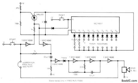
Ten independently predetermined time intervals run in sequence, with audible beep at end of each interval. Timer holds after each interval until start button is pressed to initiate next interval. If jumper is inserted, succeeding intervals start automatically. Values of R1-R9 and C determine time intervals. If same time is used for more than one step, diode outputs of those steps may be tied together to use same resistor. Supply can be in range of 5 to 18 V. Current drain is Iess than 100 μA, but increases to 40 mA during beep. Reset button can be depressed at any time, to restart timing at first intenral.-T. Henry, Ten Step Sequential Interval Timer, EDN Magazine, March 20, 1974, p 78 and 80. (View)
View full Circuit Diagram | Comments | Reading(2371)
New five-pole power tube OTL power amplifier circuit diagram
Published:2011/8/3 21:41:00 Author:Ecco | Keyword: New five-pole , power tube OTL , power amplifier

The output power can reach 50W at the 8Ω load.
(View)
View full Circuit Diagram | Comments | Reading(2106)
ELECTRONIC_CAPACITOR
Published:2009/7/16 6:07:00 Author:Jessie

Two-terminal circuit provides capacitance values from 0.1 to 100 mfd, continuously variable in three ranges. Voltage ratting is +10 v and frequency range is d-c to 45 cps. Used in low-pass RC filter with adjustable cutoff frequency, in waveform analyzer.—D.L. Bergman, Electronic Capacitor is Continuously Variable, Electronics, 38:21, p 89 (View)
View full Circuit Diagram | Comments | Reading(843)
ANTENNA_MATCHED_CRYSTAL_RADIO
Published:2009/7/12 23:44:00 Author:May

This receiver uses a tuning circuit that is, in some ways, similar to an antenna matching deviceused by amateur-radio operators to impedance-match their receiver/transmitter input/output Circuitry to the impedance of the antenna for maximum signal transfer, Inductor L2 provides a dc-signal return path for D1's output The inductance of L2 is too large to affect the circuit's tuning function. (View)
View full Circuit Diagram | Comments | Reading(1731)
IN_CIRCUIT_CAPACITOR_TESTER
Published:2009/7/16 6:06:00 Author:Jessie

Permits checking capacitors dynamically for opens or shorts without disconnecting them. Indicator light is turned on for both faults. -E. L. Major, In-Circuit Capacitor Tesler, FEE, 13;3, p 47. (View)
View full Circuit Diagram | Comments | Reading(848)
12_VDC_TO_115_VAC_AT_100_W
Published:2009/7/12 23:44:00 Author:May

566 function generator provides triangleoutput at 60 Hz with frequency stability better than ±0.02%/°C. 540 power driver feeds six-transistor power output stage. Transformer load attenuates third harmonic, giving output very close to pure 60-Hz sine wave. 566 also provides square-wave out-put for other pu rposes.- Signet Ics Analog Data Manual, Signetics, Sunnyvale, CA, 1977, p853-854. (View)
View full Circuit Diagram | Comments | Reading(1878)
| Pages:733/2234 At 20721722723724725726727728729730731732733734735736737738739740Under 20 |
Circuit Categories
power supply circuit
Amplifier Circuit
Basic Circuit
LED and Light Circuit
Sensor Circuit
Signal Processing
Electrical Equipment Circuit
Control Circuit
Remote Control Circuit
A/D-D/A Converter Circuit
Audio Circuit
Measuring and Test Circuit
Communication Circuit
Computer-Related Circuit
555 Circuit
Automotive Circuit
Repairing Circuit