
Circuit Diagram
Index 731
DIGITAL_FREQUENCY_DOUBLER_CIRCUIT
Published:2009/7/12 23:51:00 Author:May

The 74LS393 is designed to advance one count on the positive-to-negative transition of the pulse at the clock input (pins 1 and 13). An inverter in front of the B section of the counter causes the B section to advance one count on the negative-to-positive transition of the input pulse. Each section of the counter is cleared with a positive-going pulse on the master reset input (pins 2 and 12). Positive-going output pulses from pins 6 and 10 of IC2 reset the respective counters. The duration of the pulses depends upon the propagation delay of the inverters. With the 74LS04 hex inverter, delay will probably be in the vicinity of 20 to 25 ns. The output pulses are also connected to the remaining inverter gate through switching diodes and a pull-down resistor, which configures the remaining inverter as a NOR gate. The output at pin 8 of IC2 represents the input frequency multiplied by 2. (View)
View full Circuit Diagram | Comments | Reading(1841)
2_5_min_STARTING_DELAY
Published:2009/7/12 23:50:00 Author:May

Energizing of load is delayed up to 5 min after start button is pushed, as required in some CMOS circuits and digital control systems. Uses pair of 555 timers, with A operating in straightforward timing mode and B connected as set-reset flip-flop. Pushing reset button initializes system, placing A in low state and making pin 3 of B high, leaving load unenergized. When start button is pushed, A goes high and begins timing out. After delay interval, output of B goes low, energizing load until system is reset. LED can be added to indicatethattiming is in progress.-J. C. Nichols, Versatile Delay-on-Energize Timer Uses Two 555's, EDN Magazine, Oct. 5, 1975, p 76and78. (View)
View full Circuit Diagram | Comments | Reading(822)
Photo exposure timer circuit
Published:2011/8/4 3:24:00 Author:May | Keyword: Photo exposure timer

Working principle:
The photo exposure timer circuit is composed of 555 monostable circuit, which uses manually start monostable circuit. When the power is turned on, the timer will be in the steady state. At this point the voltage of the timing capacitor CT: VCT = VCC = 6V. The two inputs are in high level to this 555 equivalent trigger, that is, VS = 0. KA does not pull in, and the relay is opened, then the exposed lighting HL does not shine. This circuit provides parameters with about 1 second to 2 minutes delay time, which can be adjusted by potentiometer RP. The relay in the circuit must choose the products with the pull-in current being more than 30mA. (View)
View full Circuit Diagram | Comments | Reading(644)
METER_INDICATOR_FOR_CRYSTAL_ACTIVITY_TESTER
Published:2009/7/12 23:50:00 Author:May
A meter can be added as shown, replacing the LED in the original circuit. The meter movement should be a 0- to 1-mA type. (View)
View full Circuit Diagram | Comments | Reading(730)
THERMISTOR_COMPENSATED_ONE_SHOT
Published:2009/7/16 11:58:00 Author:Jessie

Negative-temperature-coefficient thermistor in pulse width determining network keeps pulse width of mvbr constant within 0.6% over range of 25℃. Basic period with values shown is 357 microsec, increasing to 359 microsec at temperature extremes.-B. Hedin, Temperature-Compensated One-Shot, EEE, 12:5, p 75. (View)
View full Circuit Diagram | Comments | Reading(549)
50_KC_FREE_RUNNING_MVBR
Published:2009/7/16 11:55:00 Author:Jessie

Uses 2N1304 transistors having base-emitter breakdown of -25 V, making emitter diodes unnecessary.-Texas Instruments Inc., Transistor Circuit Design, McGraw-Hill, N.Y., 1963, p 380. (View)
View full Circuit Diagram | Comments | Reading(650)
QUARTZ_CRYSTAL_SPECIFICATIONS
Published:2009/7/12 23:49:00 Author:May


Five main parameters control the characteristics of a crystal, as noted in the equivalent circuit for the figure. These parameters are:
● C1, the motional capacitance● L1, the motional inductance● R1, the equivalent series resistance (ESR)● C0, the parallel capacitance resulting from the electrodes and crystal packaging● CL, external load capacitanbe of the circuit
C1 and L1 are interdependent because they determine the resonant frequency of the crystal. If we know one of the parameters, we can readily compute the other if we know the series resonant frequency. R1 is the resistance determined by the motional (piezoelectric) behavior of the crystal. If it is too high, the crystal might not start oscillation. C0 is a physical capacitor, created by the electrodes plated onto the crystal surface, along with some additional capacitance from the package. Generally, larger C0 contributes to better pullability. CL is the load capacitance of the user's circuit. The crystal must operate at the right frequency in the intended circuit, so this value needs to be included in the crystal purchase specification. (View)
View full Circuit Diagram | Comments | Reading(1098)
ADJUSTABLE_DUTY_CYCLE_MONO
Published:2009/7/16 11:54:00 Author:Jessie

When ratio of pulse width to pulse spacing exceeds value set by R12, width of output pulse is automatically reduced to maintain duty cycle at preset maximum. Used as pulse driver for high-power amplifier when duty cycle must be limited to prevent overheating. If duty cycle is set for 50% and frequency is increased, output will be square wave for all frequencies up to maximum frequency limit for circuit. R9 adjusts output pulse width from 0.7 to 7 microsec.-D. N. Lee, Monostable Multi With Adjustable Duty Cycle, EEE, 13:9, p 92-94. (View)
View full Circuit Diagram | Comments | Reading(741)
Y_POSITION_DETECTOR_FOR_MISSILE_TRACKER
Published:2009/7/16 11:31:00 Author:Jessie
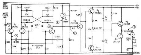
Flip-flop Q2-Q3 is triggered by processed video pulse fed through Q1and by delay vertical sync pulse fed through Q4. Width of flip-flop output pulse, relate to target position is integrated by Q6-Q7 and amplified by Q8-Q9 to give d-c output voltage proportional to Y-position of target. –T. L. Poppelbaum,TV Camera Tracker: Can it Detect Missile Decoys? Electronics, 36:17, p 51-55. (View)
View full Circuit Diagram | Comments | Reading(817)
TRANSISTORIZED_FREE_RUNNING_CASCODE_MULTIVIBRATOR
Published:2009/7/16 11:27:00 Author:Jessie

Output waveform can be rectangular or sawtooth, with polarity depending on setting of potentiometer. -C. Sing, Advantages of Free-Running Cascade Multivibrators, Electronics, 37:5, p 28-29. (View)
View full Circuit Diagram | Comments | Reading(853)
WIDE_RANGE_MONO
Published:2009/7/16 11:26:00 Author:Jessie

Adding one transistor(Q6)to linear one-shot increases frequency range 150 times.-G. Marosi, Wide Range Monostable Multivibrator, EEE, 13:9, p 76. (View)
View full Circuit Diagram | Comments | Reading(650)
EMITTER_COUPLED_ASTABLE_LOGIC_DRIVER
Published:2009/7/16 11:23:00 Author:Jessie

Self-starting design gives good frequency stability along with high-speed saturated positive and/or negative outputs. Current-mode logic output is optional, being obtained when circuit Q3-Q4 in dashed box is replaced by circuit of Q5. C1 determines operating frequency in range from 50 cps to 8.5 Mc.-D. R. Hoppe, Emitter-Coupled As-table With Saturated Output, EEE, 14:7, p 106. (View)
View full Circuit Diagram | Comments | Reading(800)
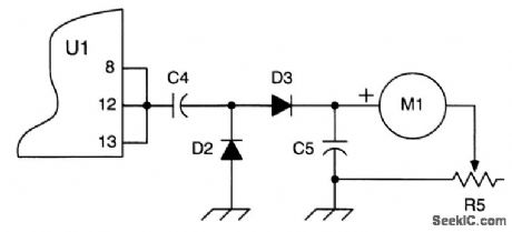
CRYSTAL_ACTIVITY_TESTER
Published:2009/7/12 23:47:00 Author:May
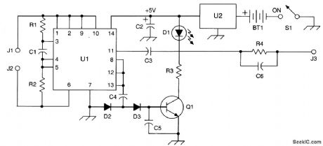
U1 is a 74LS00 quad two-input NAND-gate logic chip.The bo LS version was selected because ofits low current requirement Two of its internal gates are connected as inverters and,In conjunction with R1,R2,and C1,form a crystal oscillator when a crystai is connected between J1 and J2 The third gate,also connected as an inverter,is used as a buffer to provide RF at the crystalfrequency from pin 11,through isolation capacitor C3 and high-pass filter R4 and C6,to J3 so that the crystal frequency can bemonitored by an external-frequency counter The fourth gate,also connected as an inverter-buffer,provides RF at the crystal frequency from puts 8,12,and 13 connected in parallel The RF is fed through isolation capacitor C4 to voltage-doubling rectifiers D2 and D3,and the resulting dc voltage is filtered by C5 and provides a positive bias to the base of Q1,an NPN transistor,which is normally cut off.Q1 goes into conduction, and its collector current flows through LED D1 and R3 in serles,both forming the collector load circuit. The greater the activity of the crystal, the higher the positive bias on the base of Q1 will be, and the higher its collector current will be. This current illuminates D1, and its relative brightness is indicative of the level of crystal activity. (View)
View full Circuit Diagram | Comments | Reading(2442)
VARIABLE_POWER_ONE_SHOT
Published:2009/7/16 10:55:00 Author:Jessie

Switches load currents from few ma to over 1 amp for precise time interval ranging from few millisec to one minute. Is excellent solid-state substitute for slug relays, dashpots, and thermal timers. Several stages can be cascaded to form sequence timer. With values shown, and RT at 680K, 1-V trigger pulse initiates 1-sec on period.-J. C. Rich and R. D. Turner, Variable Time, Power One-Shot Multivibrator, EEE, 12:7, p 25-26. (View)
View full Circuit Diagram | Comments | Reading(718)
SINGLE_COIL_ORYSTAL_RADIO
Published:2009/7/12 23:45:00 Author:May

A starting setup for this circuit is as follows:Connect the antenna to the second tap up from the bottom of the coil (that's the end of the coil that's connected to ground). The diode should connect to about the fourth tap up from the bottom, and C1 should be attached to the seventh tap or so up from the bottom. Those tap positions might not be the best starting point for your antenna/ground arrangerttent. That doesn't matter, however, because to obtain the best results with the receiver at your location, you should experiment with all variables anyway. (View)
View full Circuit Diagram | Comments | Reading(1365)
REDUCING_RESET_POWER_LEVEL
Published:2009/7/16 10:53:00 Author:Jessie

Addition of diode D1 to conventional mvbr decreases required amplitude and duration of reset pulse. -H. Inose and T. Tomiyama, Diode Lowers Multi's Reset Power Level, Electronics, 39:13, p 76-77. (View)
View full Circuit Diagram | Comments | Reading(687)
FAST_RECOVERY_ONE_SHOT
Published:2009/7/16 10:49:00 Author:Jessie

Dynamic period can be varied linearly over range of 20 to 425 microsec. Retrigger time is only 3 microsec for short periods and 14 microsec for longest periods. Circuit is conventional except for d-c isolation diode D1 and drive resistor R4.-R. S. Hughes, A linear, Voltage-Variable One-Shot With Fast Retrigger Time, EEE, 13:5, p 78-79. (View)
View full Circuit Diagram | Comments | Reading(759)
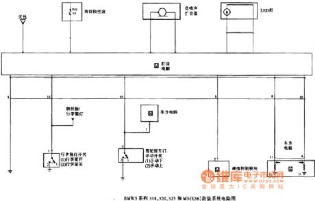
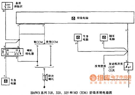
BMW3 series 318,320,325 and M3(E36) anti-theft system circuit 3
Published:2011/7/19 10:37:00 Author:Nancy | Keyword: BMW3 series, anti-theft system
View full Circuit Diagram | Comments | Reading(532)
BMW3 series 318,320,325 and M3(E36) anti-theft system circuit 2
Published:2011/7/19 10:38:00 Author:Nancy | Keyword: BMW3 series, anti-theft system
View full Circuit Diagram | Comments | Reading(493)
CONTINUOUSLY_VARIABLE_PRR
Published:2009/7/16 10:46:00 Author:Jessie

When basic mvbr is biased from constant-current source, tops of square wave become flat across collector resistor, and triangular wave across capacitor becomes linear. Pulse repetition rate then varies directly with magnitude of constant biasing current, over range of 5.6 cps to 2.68 Mc, by using only seven different capacitance values for C (from 330 pf to 100 mfd).-J. H. Bayne, Jr., and R. J. Haislmaier, Improved Multi with Continuously Variable Rep Rate, EEE, 13:5, p 44-45. (View)
View full Circuit Diagram | Comments | Reading(859)
| Pages:731/2234 At 20721722723724725726727728729730731732733734735736737738739740Under 20 |
Circuit Categories
power supply circuit
Amplifier Circuit
Basic Circuit
LED and Light Circuit
Sensor Circuit
Signal Processing
Electrical Equipment Circuit
Control Circuit
Remote Control Circuit
A/D-D/A Converter Circuit
Audio Circuit
Measuring and Test Circuit
Communication Circuit
Computer-Related Circuit
555 Circuit
Automotive Circuit
Repairing Circuit