
Circuit Diagram
Index 729
AXIS_CROSSING_DETECTOR
Published:2009/7/16 20:31:00 Author:Jessie
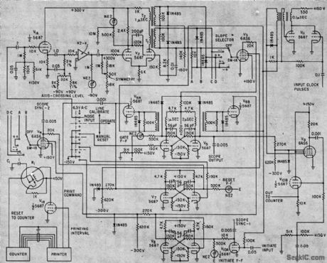
Used in weak-signal detectors and in theoretical studies of noise.Samples time intervals between positive-going and negative going zero crossings, to establish un interval gate whose width equals time interval of desired weak signal. Output goes to cro for viewing of interval gate.-A. J. Rainal, Digital Measurement Axis-Crossing Intervals,Electronics, 33:23, p 88-91. (View)
View full Circuit Diagram | Comments | Reading(758)
BATTERY_SAVING_TIMER
Published:2009/7/13 1:32:00 Author:May

Developed for use with alarms, remote controls, or unattended electronic equipment, to turn off battery auto-matically at predetermined interval after circuit is actuated by control logic or switch. Turn-on applies positive pulse that triggers SCR on, grounding load and UJT timer Q2. After delay interval determined by values of C1 and R1, Q2 fires and discharges C1, producing pulse across R, that tums on Q3. This in tum shunts SCR and commutates it off. Circuit is thus turned off, after which only very small leakage currents through reverse SCR junction will be drain on battery.-D. Weigand, Battery Saver Has Automatic Tum-Off, EDN Magazine, April20, 1973, p91. (View)
View full Circuit Diagram | Comments | Reading(694)
JET_AUTOPILOT_CONTROL
Published:2009/7/13 1:31:00 Author:May

Adder-attenuator amplifier decreasos gain slowly, allowing new control modes to be set up without un-desirable aircraft motion or bumps, when jct pilot changes to different flight control mode, as from mach control to attitude control or altitude control. Relay KB allows new new mode to be set up, and output then increases to normal. When pilot operates fading switch (not shown), relay contact KA closes and 90V d-c is applied to fading circuit. Fadeout time constant is 0.5 sec and fade-in time constant 0.3 sec.-L. D. Fry, Taking the Bumps Out of Automatic Flight Control, Electronics, 32:32, p106-109. (View)
View full Circuit Diagram | Comments | Reading(829)
HIGH_VOLTAGE_FOR_PORTABLE_CRO
Published:2009/7/16 20:28:00 Author:Jessie

Derives 3.3 kv for post-accelerating anode from 20-kc high-voltage oscillator supply.-O. Svehcug and J. R. Kobbe, Banery-Operated Transistor Oscilloscope,Electronics, 33:12, p 80-83. (View)
View full Circuit Diagram | Comments | Reading(1045)
DUAL_FUNCTION_BISTABLE_SCRAM
Published:2009/7/13 1:19:00 Author:May

Porlion at right of dotted lines acts as regulator that holds constant voltage on output circuit until tripping of control rods is called for by nuclear radiation detector.Outputs of bistable circuits are connected through and gates so that, if desired, two input signals are necessary before trip signcd is generated. Malfunction in ion chambers or failure of circuit component can make reactor exceed maximum critical assembly condition and generate trip signal that drops control rods.-E. J.Wade and D.S. Davidson, How Transistor Circuits Protect Atomic Reactors, EJectronics, 31:29,73-75. (View)
View full Circuit Diagram | Comments | Reading(976)
DEFLECTING_22_INCH_CRT_AT_50_KC
Published:2009/7/16 20:26:00 Author:Jessie


Circuit provides 5-amp peak-to-peak yoke current for full 70°defleaction of analog computer display. Rapid collector turnoff minimizes retrace lime. two B-211 diodes,series-connected as dampers,must be matched for voltage division.-R.S. Hartz and R. C. Allen, Reliable Circuit Supplies High Peak Deflection Voltages:EIectronics, 35:41,p 54-55. (View)
View full Circuit Diagram | Comments | Reading(880)
AUTOPILOT_GYRO_CONTROL
Published:2009/7/13 1:11:00 Author:May

Flip-flop Q1-Q2 controls breakdown of zener diode D2. At breakdown, D2 has low impedance, shunting 180,000-ohm trigger resistor and reducing input to five-stage d-c amplifier Q3-Q7. Over-all voltage gain is 27. Demodulator is bistable lip-lop Q11-Q12 and series switching transistors Q8-Q9, giving no-signal d-c output of 9V. This level is modulated 3V for maximum in-phase or out-of-phase error signals from gyros.-J. H. Porter, Miniaturized Autopilot System for Missiles, Electronics, 33:43, p60-64. (View)
View full Circuit Diagram | Comments | Reading(1002)
TWO_SIGNAL_DISPLAY
Published:2009/7/16 20:23:00 Author:Jessie

Electronic switch samples two video signals and modulates crt beam so both waveforms appear simultaneously on screen. Matched diodes D1 and D2 serve as switches for the positive 2-v video signals.-A. E. Popodi,Reliable Repertoire Of Display Circuits, Electronics 38:2, p 60-66. (View)
View full Circuit Diagram | Comments | Reading(950)
TWO_TERMINAL_PIEZO_DEVICE_DRIVER
Published:2009/7/13 0:09:00 Author:May
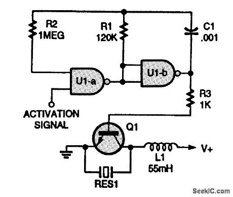
Two-terminal devices can be driven by two NAND gates. A booster coil is used to compensate for the sound-pressureattenuation caused by the case. (View)
View full Circuit Diagram | Comments | Reading(805)
CRO_SWEEP_TRIGGER
Published:2009/7/16 20:22:00 Author:Jessie

Base of Q1 is grounded once during each revolution by commutator segment of gyro balancer, to make circuit produce sharp pulse that triggers oscilloscope sweep.-F. W. Kear, Electronic System for Balancing Gyro Wheels, Electronics, 33:43, p 82-85. (View)
View full Circuit Diagram | Comments | Reading(973)
CRO_LEVEL_CONTROLLED_STROBE
Published:2009/7/16 20:20:00 Author:Jessie

Variable input level determines part of telemetry signal that is selected for cathode-ray display.Output of Schmitt trigger Q2-Q3 is square wave with repetition rate determined by time-base frequency, and mark-space ratio controlled by variable d-c level input.-A. D. Runnalis, Bluebird Racer's Telemetry System,Electronics, 33:44, p 70-72. (View)
View full Circuit Diagram | Comments | Reading(784)
LOW-DISTORTION_LINE_DRIVER
Published:2009/7/13 0:06:00 Author:May
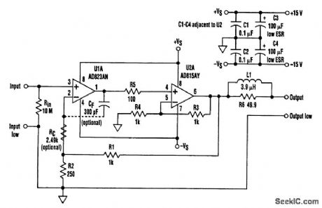
This low-distortion driver circuit delivers up to ±0.5 A and is suitable for loads of 10Ω and up. Using a low-offset, low-bias-current input stage, the driver can be entirely direct-coupled. Gain is equal to 1+R2/R1. (View)
View full Circuit Diagram | Comments | Reading(814)
TRANSIENT_ELIMINATOR
Published:2009/7/13 0:06:00 Author:May


Used between DC power supply and load to eliminate supply transients that might damage semiconductor devices. Zener rating should be about 10% higher than supply voltage so Q1 is normally turned off. Q2 is normally conducting. When voltage spike is present on input line, zener conducts and turns Q1 on. Q1 then places positive bias on 10K pot to turn off Q2 and protect load during transient.-J. Fisk, Circuits and Techniques, Ham Radio, June 1976, p 48-52. (View)
View full Circuit Diagram | Comments | Reading(967)
PROGRAMMABLE_CURRENT_SOURCE
Published:2009/7/13 0:04:00 Author:May

Constant-current Sources are required in many applications,particularly when it comes to battery charging in such applications,it is desirable that the output current be accurate,temperaturestable,and adjustable The controller also can be successfully employed as the control element in a low-cost linear current source.Output current is sensed by resistor R1,with the value selected so that 100 mV is full-scale The voltage across R1 is amplified by a factor of 10 and averaged across capacitor C4.AN internal transconductance error amplifier compares the voltage on pin 8 against the programming voltage at pin 7.The error-amplifier outputis present on pin 2 (Iout),and is level-shiftedby Q2 to control the PNP pass transistor Output current is programmed by adjusting the voltage across R5 (1 V full-scale).The LT1121 LDO regulator provides a 5-V,±1.5 percent reference voltage so that current can be accurately programmed by simply connecting different values for Rprog. The input voltage can range from +6 to +28 V, with output current changing less than 0.3 percent Properheat sinking must be provided for Q1, especially when operating with large input-to-output voltage differentials.Transistor Q3 and R4 limit the magnitude of Q1's base drive during dropout,preventing excessive dissipation in driver transistor Q2 using voltage regulator IC2, the constant-currentSource operates directly from the unregulated input voltage. Pulling IC2's shutdown ptn lowturns off VCC to the entire circuit,and limits the reverse current drawn from the output to less than 25μA. (View)
View full Circuit Diagram | Comments | Reading(2995)
BMW7 series 740i E38DWA IV anti-theft system circuit
Published:2011/7/19 10:28:00 Author:Nancy | Keyword: anti-theft system , BMW7 series

View full Circuit Diagram | Comments | Reading(785)
SPARK_MACHINING_SERVO_DRIVE
Published:2009/7/13 0:03:00 Author:May
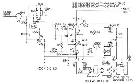
Posilioning information is derived from gap voltage, fed to integrating circuit through diode V1, and resuhing output fed through V2 to cath-ode-coupled push-pull d-c amplifier that excites field of amplidyne generator to move tool electrode toward or away from work-piece, as required to permit sparkover at voltage selected for machining conditions desired. Used chiefiy for work on high-tempemture alloys and otherwise unmachinoble materials.-E. M. Williams and C. P. Porterleld, Spark Machine Tool has Servo Control, Electronics,31:43,p90-92. (View)
View full Circuit Diagram | Comments | Reading(1183)
TEAl504 switching power control circuit diagram
Published:2011/8/4 2:14:00 Author:Ecco | Keyword: switching power control
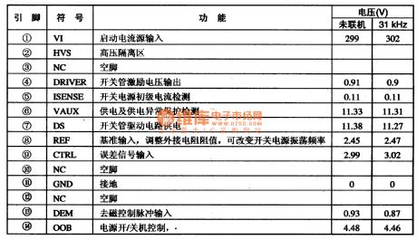
TEAl504 new switching power supply control IC produced by Philips, which is the core component to form the separately excited switching power supply, and they are widely used in color television sets, computers and color monitors, and other electrical power supply circuits. TEA1504 integrated circuit includes start-up circuit, switch drive circuit, power supply circuit, oscillation frequency control circuit, power on / off control circuit, switch circuit incentives, and other auxiliary circuits.
(View)
View full Circuit Diagram | Comments | Reading(578)
CONSTANT_CURRENT_SOURCE_CONVERTER
Published:2009/7/13 0:03:00 Author:May

To maintain regulation, the switching voltage regulator shown includes independent loops of current and voltage feedback. If the voltage loop is disabled, the current loop can be used to implement a general-purpose current source. The first step in obtaining a current source is to apply 5 V to V+. Because the chip expects 12 V of feedback at that terminal, it assumes a loss of regulation and shifts control to the current loop. This mode of operation allows an increasing ramp of current through Q1, causing the voltage at pin 8 to increase until it reaches the internal comparator threshold (210 mV). Timing circuitry then turns off Q1 for a fixed 2.3 μs, and the cycle repeats. The result is a relatively constant inductor current, which also happens to be the load current.With a proper choice of component values, the circuit generates constant current over a wide range of input voltages. The circuit (with component values shown) is a fast charger for NiCd batteries that provides 60-mA charging currents. (View)
View full Circuit Diagram | Comments | Reading(2120)
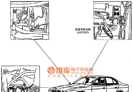
BMW7 series anti-theft component location circuit
Published:2011/7/19 10:30:00 Author:Nancy | Keyword: BMW7 series, anti-theft , component location
View full Circuit Diagram | Comments | Reading(584)
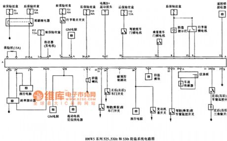
BMW5 series 525,530it and 530t anti-theft system circuit 3
Published:2011/7/19 10:31:00 Author:Nancy | Keyword: BMW5 series, anti-theft system
View full Circuit Diagram | Comments | Reading(475)
| Pages:729/2234 At 20721722723724725726727728729730731732733734735736737738739740Under 20 |
Circuit Categories
power supply circuit
Amplifier Circuit
Basic Circuit
LED and Light Circuit
Sensor Circuit
Signal Processing
Electrical Equipment Circuit
Control Circuit
Remote Control Circuit
A/D-D/A Converter Circuit
Audio Circuit
Measuring and Test Circuit
Communication Circuit
Computer-Related Circuit
555 Circuit
Automotive Circuit
Repairing Circuit