
Circuit Diagram
Index 737
TTL_ORYSTAL_OSCILLATOR
Published:2009/7/12 23:28:00 Author:May

Here is an oscillator circuit that uses no L/C components. It uses two sections of a 7400 TTL IC, two resistors, and a crystal to make up a simple and stable oscillator circuit. (View)
View full Circuit Diagram | Comments | Reading(2916)
CALIBRATOR_FOR_PORTABLE_CRO
Published:2009/7/16 21:15:00 Author:Jessie

Generates 40-mv square wave at 2 kc. Provides swing of 30 v at each crt deflection plate.-O. Svehaug and J. R. Kobbe, Battery-Operated Transistor Oscilloscope,Electronics, 33:12, p 80-83. (View)
View full Circuit Diagram | Comments | Reading(1190)
GYRO_VIBRATION_AMPLIFIER
Published:2009/7/16 21:15:00 Author:Jessie
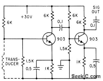
Vibration resulting from imbalance is sensed by inductive transducer that produces sine wave which is amplified by circuit and displayed on cro.-F.W. Kear,Electronic System for Balancing Gyro Wheels, Electronics, 33:43, p 82-85. (View)
View full Circuit Diagram | Comments | Reading(808)
32768_kHz_MICROPOWER_OSCILLATOR
Published:2009/7/12 23:27:00 Author:May

Using an LTC1441, this oscillator pulls 9 μA at a supply voltage of 2 V. The circuit has no spurious modes. (View)
View full Circuit Diagram | Comments | Reading(1387)
GaAsFET_BIAS_SUPPLY_1
Published:2009/7/16 21:14:00 Author:Jessie

The LTC1550 and LTC1551CS8-4.1 are switched-capacitor voltage inverters that generate a regulated -4.1-V output at up to 20-mA load current. An internal linear postregulator reduces the out-put-voltage ripple to less than 1 mV, making the LTC1550 and LTC1551CS8-4.1 excellent for use as bias-voltage generators for transmitter GaAsFETs in portable RE and cellular telephone applications. The single supply voltage can range from 4.5 to 6.5 V (7 V absolute maximum). The charge pump uses four small external capacitors and operates at 900 kHz, eliminating interference with the 400-to 600-kHz IF signals commonly used in RF systems. (View)
View full Circuit Diagram | Comments | Reading(727)
12_VDC_TO_115_VAC_AT_400_Hz
Published:2009/7/12 23:27:00 Author:May
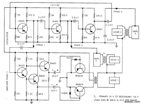
Provides threephase output at 20 W by using RC coupling to oscillator in such a way that 120°phase difference exists at collectors of 2N651 transistors of oscillator. Emitter-follower amplifier driving push-pull power output transistors is shown only for phase 1; other two phases use similar amplifiers, Power transistors are operated in saturated switching mode.-R. J. Haver, The ABC's of DC to AC Inverters, Motorola, Phoenix, AZ, 1976, AN-222, p 15. (View)
View full Circuit Diagram | Comments | Reading(1253)
VOLTAGE_PROGRAMMABLE_CURRENT_SOURCE
Published:2009/7/16 21:14:00 Author:Jessie

This circuit is a programmable current source in which op amp LT1102 (Linear Technology Corp.) is used in conjunction with LT1006 op amp. A1, biased by Vin, drives current through R (10Ω) and the load. A2 senses this current and controls A1. The 10-kΩ resistor and 0.05-μF capacitor sets the frequency response of the circuit.
(View)
View full Circuit Diagram | Comments | Reading(3598)
PULSE_HEIGHT_DISCRIMINATOR
Published:2009/7/16 21:14:00 Author:Jessie

Delivers trigger pulse when input signal reaches pre determined threshold. Used in nuclear counting experiments, in satellite and rocket applications where sensitivity and stability are essential.-R. Ii. Wagner, Stable, Sensitive Pulse Height Discriminator, EEE, 10:7, p 28-29. (View)
View full Circuit Diagram | Comments | Reading(1067)
0_5_min_DELAY
Published:2009/7/12 23:27:00 Author:May
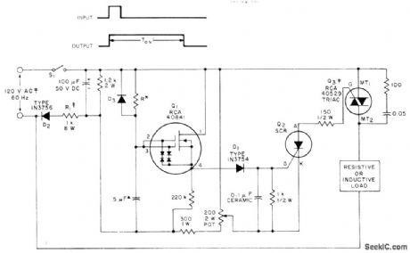
Value of resistor R controls duration of time delay provided by RCA 40841 dual-gate FET in SCR trigger circuit, with SCR in tum serving to triggertriacfor handling highcurrent resistive or inductive AC loads. Maximum delay of 5 min is obtained when R is 60 megohms (IRC type CGH or equivalent resistor). Timing is accurate within 10% over temperature rangeof -25℃to +60℃. D3 should be rated 60 V Use any SCR capable of handling triactrigger current,rated 60 V.- Linear Integrated Circuitsand MOS/FET,s, RCA Solid State Division,Somerville,NJ,1977,p435-437. (View)
View full Circuit Diagram | Comments | Reading(2181)
BASIC_NE602_COLPITTS_CRYSTAL_OSCILLATOR
Published:2009/7/12 23:26:00 Author:May

This basic Colpitts crystal oscillator will work with fundamental-mode crystals up to 20 MHz. (View)
View full Circuit Diagram | Comments | Reading(1369)
13_GHz_ATV_TRANSMITTER
Published:2009/7/12 23:25:00 Author:May
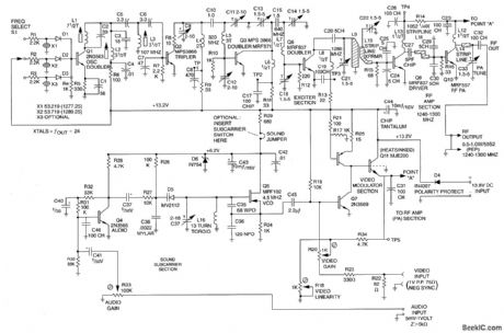

This TV transmitter operates from a +12-Vdc source and produces about 1 W peak power on sync tips. Output frequency is 1240 to 1300 MHz, but operation is possible to 1325 MHz (for U.K.band). Video interface is 1 V p-p/75 Ω negative sync; audio is 5 mV to 1 V @ 255 kΩ. For PAL operation, reduce the number of turns on L16 to 11 for 5.5-MHz sound.A kit of parts for this transmitter is available from North Country Radio, P.O. Box 53, Wykagyl Station, New Rochelle, NY 10804-0053A. (View)
View full Circuit Diagram | Comments | Reading(2884)
DIGITAL_VOLTMETER_CIRCUIT
Published:2009/7/16 21:14:00 Author:Jessie

A basic digital voltmeter circuit using the Harris Semiconductor ICL7107 is shown. It has a 2-V range. Calibration consists of applying a known voltage of 1.2 V to the input and adjusting R3 for a correct reading on the display. Supply is ±5 V, and S1 selects either the supply voltage or an external reference. (View)
View full Circuit Diagram | Comments | Reading(5534)
DIGITAL_LOGIC_FREQUENCY_DOUBLER
Published:2009/7/12 23:25:00 Author:May

This circuit can be used if very high frequency operation is needed, or if very narrow output pulses can be tolerated. The output pulse width is determined by the propagation time delay of the exclusive-OR gate, and the input frequency cannot exceed 1/2(delay). (View)
View full Circuit Diagram | Comments | Reading(7095)
TRANSFORMERLESS_POWER_SUPPLY
Published:2009/7/16 21:13:00 Author:Jessie

By selecting capacitors, various voltages can be obtained from this supply. Notice that C2 through C7 must be nonpolarized capacitors, such as oil-filled or foil types (Mylar) rated for at least 250 Vac.
Warning: This supply is not isolated from the ac mains and presents a serious safety hazard if body contact is made anywhere to this circuit or anything that is powered by it. Use only for applications where contact is avoided or impossible. (View)
View full Circuit Diagram | Comments | Reading(1973)
NE602_ADJUSTABLE_ORYSTAL_OSCILLATOR
Published:2009/7/12 23:25:00 Author:May

Here, a variable capacitor is added to the circuit to make it easier to obtain the desired frequency. (View)
View full Circuit Diagram | Comments | Reading(879)
33_V_7_A_SUPPLY
Published:2009/7/16 21:12:00 Author:Jessie

Many microprocessor systems use 3.3-V microprocessors, cache RAM, and chip sets. This system configuration increases the current requirements of the 3.3-V supply. In addition, many of these microprocessors have a stop-clock feature for power savings, which introduces a load-current step to the power supply. Adjustable regulators are recommended for microprocessors that have power-saving (stop-clock) modes. The circuit shown has good transient response to load steps for most 3.3-V microprocessors. An external capacitor at the ADJUST pin can reduce the total filter capacitance required by one half to take care of large load transients. (View)
View full Circuit Diagram | Comments | Reading(680)
SWITCH_SELECTED_FIXED_VOLTAGE_POWER_SUPPLY
Published:2009/7/16 21:12:00 Author:Jessie


This supply can serve as a battery eliminator for various devices (such as tape recorders, small radios, clocks, etc.).
S1 selects a resistance that is predetermined to provide a preselected output voltage. In this circuit, various conunonly used supply voltages produced by batteries were chosen, but any voltages up to the rating of T1 (approximately) can be produced by choosing an appropriate resistor.
The resistor value is given by:
Remember to provide adequate heatsinking for U1. (View)
View full Circuit Diagram | Comments | Reading(913)
FLASH_MEMORY_Vpp_GENERATOR
Published:2009/7/16 21:12:00 Author:Jessie

Generating 12 V for flash memory programming is a common requirement in portable systems and PCMIA cards. The LT1109-12 dc-to-dc converter simplifies this task and uses only 0.75 in2 of PC board space. The LT1109-12 is offered in an eight-lead SO package and requires only three other surface-mount components to construct a complete 12-Vpp generator. At 12 V, 60 mA of programming current is produced, enough for simultaneous programming of two flash memories. The circuit draws 320 μA (max.) of standby current while shut down and provides a clean transition from 5 to 12 V at its output with no overshoot. (View)
View full Circuit Diagram | Comments | Reading(787)
MICROSECONDS_TO_HOURS_1
Published:2009/7/12 23:21:00 Author:May


Simple CMOS circuit serves as time-delay switch and generalpurpose timer. Gated oscillator and latch are obtained from CD4001 quad two-input NOR gate, and 14-stage counter uses CD4020. TON is function of oscillator frequency as determined by RXCX and proper 2N output from counter. Pulse applied to latch input enables oscillator and counter. Latch output remains high until counter resets latch at end of count selected by switch. Further decoding is required for count or time variations finer than power of 2.-J.Chin, Low-Power Counter is Programmable over Wide Range, EDN Magazine, March 20, 1974, p 83. (View)
View full Circuit Diagram | Comments | Reading(2641)
PORTABLE_CRO_HORIZONTAL_AMPLIFIER
Published:2009/7/16 21:12:00 Author:Jessie

Balanced circuit includes temperature compensation. Closing S1 provides magnification of 5 on screen. Bandwidth is 1 Mc.-O. Svehaug and J. R. Kobbe, Battery-Operated Transistor Oscilloscope, Electronics, 33:12, p 80-83. (View)
View full Circuit Diagram | Comments | Reading(821)
| Pages:737/2234 At 20721722723724725726727728729730731732733734735736737738739740Under 20 |
Circuit Categories
power supply circuit
Amplifier Circuit
Basic Circuit
LED and Light Circuit
Sensor Circuit
Signal Processing
Electrical Equipment Circuit
Control Circuit
Remote Control Circuit
A/D-D/A Converter Circuit
Audio Circuit
Measuring and Test Circuit
Communication Circuit
Computer-Related Circuit
555 Circuit
Automotive Circuit
Repairing Circuit