
Circuit Diagram
Index 738
NE602_THIRD_OVERTONE_CRYSTAL_OSCILLATOR
Published:2009/7/12 23:20:00 Author:May

This overtone crystal oscillator uses thirdovertone crystals and will work from 25 to 50 MHz. (View)
View full Circuit Diagram | Comments | Reading(1080)
VOLTAGE_MONITOR
Published:2009/7/16 21:11:00 Author:Jessie

When voltages are measured, it is not always necessary to find the exact value. Often, it is sufficient to check whether a potential lies within a certain range of voltages. The present circuit indicates by means of three LEDs whether a voltage is greater than 4 V, 5.7 V, or 7.4V. The reference potential is provided by a series network of diodes D4 to D9. The LEDs are connected to various junctions in this network. The measurand is applied to the LEDs via emitter follower T1 and series resistors. Any one LED will light only if the input voltage exceeds the sum of the base-emitter junction of T1, the drop across the relevant series resistor, the LED voltage, and the drop across the diodes following the LED. (View)
View full Circuit Diagram | Comments | Reading(1)
BMW3 series central control component location circuit
Published:2011/7/19 10:45:00 Author:Nancy | Keyword: BMW3 series , central control , component location
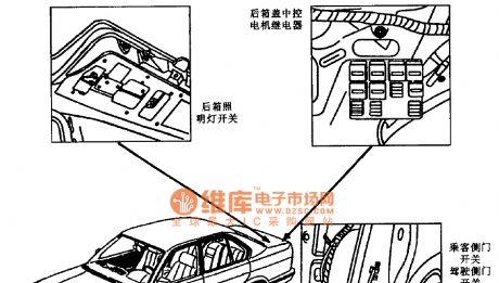
View full Circuit Diagram | Comments | Reading(414)
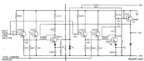
TRACE_INTENSIFIER
Published:2009/7/16 21:11:00 Author:Jessie

Designed to convert weak positive-going pulse lo negative-going pulse with 15 v minimum amplitude, as required on cathode of A-scope radar presentation on commercial oscilloscope. Minimum input amplitude is 250 mv.-L.J. Brocato, Scope-Trace Intensification Converter,EEE,13:2,p 62-63. (View)
View full Circuit Diagram | Comments | Reading(721)
ON_OR_OFF_CONTROL
Published:2009/7/12 23:19:00 Author:May

Circuit shows two ways of connecting 555 timer IC, for switching load on or switching load off at end of timing interval determined by setting of 5-megohm pot (1 to 60 s) and initiated by manual start switch. If desired, both loads can be connected to circuit for simultaneous switching.-E. R. Hnatek, Put the IC Timer to Work in a Myriad of Ways, EDNMagazine, March 5, 1973, p 54-58. (View)
View full Circuit Diagram | Comments | Reading(640)
SCR_VARIABLE_dc_POWER_SUPPLY
Published:2009/7/16 21:11:00 Author:Jessie

By adjusting the SCR trigger point, a form of phase control can be obtained from an SCR, which produces a dc output, depending on the conduction angle. (View)
View full Circuit Diagram | Comments | Reading(1369)
PULSE_HEIGHT_DISCRIMI_NATOR
Published:2009/7/16 21:11:00 Author:Jessie
Selected pulses pass through timing gate Q7 (open for fixed time) to counter that registers average intensity of solar radiation falling in give wavelength band.-J. Ackroyd, Orbiting Spectrometer Plots Solar X-Rays, Electronics, 34:43, p 55-57. (View)
View full Circuit Diagram | Comments | Reading(667)
NE602_OVERTONE_ORYSTAL_OSCILLATOR
Published:2009/7/12 23:18:00 Author:May

For higher frequencies, use an overtone crystal oscillator like the one shown here. The circuit is a Butler oscillator. The overtone crystal is connected between the oscillator emitter of the NE602 (pin 7) and a capacitive voltage divider that is connected between the oscillator base (pin 6) and ground. An inductor is also in the circuit (L1),and it must resonate with C1 to the overtone frequency of crystal XTAL1. The circuit can use either third- or fifth-overtone crystals up to about 80 Fig. 24-4 MHz. (View)
View full Circuit Diagram | Comments | Reading(2373)
STEP_VARIABLE_dc_SUPPLY
Published:2009/7/16 21:10:00 Author:Jessie

Intended as a replacement for generally poorly regulated wall-type ac/dc adapters, this circuit offers superior performance to simple, unregulated adapters. Voltages of 3, 6, 9, and 12 V are available. The DPDT switch serves as a polarity-reversal switch. R2 through R6 can be replaced with a 2.5-kΩ pot for a variable voltage of 1 to 12 V. R7 through R10 can be replaced by a fixed resistor of about 1 kΩ if the LED1 brightness variation with output voltage is not a problem. (View)
View full Circuit Diagram | Comments | Reading(696)
AC_LINE_VOLTAGE_MONITOR
Published:2009/7/16 21:09:00 Author:Jessie

This figure shows the schematic of the ac line-voltage monitor circuit. The circuit receives 12 Vdc from a wall transformer. The circuit is centered around two quad LM324 op-amp ICs (IC1 and IC2) that receive regulated operating power from a clamped portion of the dc supply provided by a 5.1-V zener diode, D3. The op amps drive an LED bar graph, consisting of LED1 through LED7. The op amps receive an adjustable reference voltage from the center contact of potentiometer R16 and an input voltage from the voltage divider, consisting of resistors R1, R2, R4, R6, R8, R10, R12, and R18. Those resistor values were chosen so that the op-amp outputs sequentially turn on and light the LEDs as the ac line voltage, or one-tenth of it, varies from 100 to 132 V. Potentiometer R16 sets the midpoint of the LED bar graph-usually 118 V-which can be shifted, if you like. (View)
View full Circuit Diagram | Comments | Reading(5406)
UHF_ATV_DOWNCONVERTER_FOR_900_AND_1300_MHz
Published:2009/7/12 23:18:00 Author:May

This clownconverter is tunable and can cover either 902 to 928 MHz or 1240 to 1300 MHz for receiving amateur television transmissions or other wideband signals. An NEO 25139low-noise RE am-plifier feeds a BFR90 mixer driven by a BFR tunable LO operating 61 or 67 MHz below the received frequency. A pair of 2N3563 transistors are used as a post-IF amplifier. Overall gain is 37 to 40 dB with around 1.5-dB noise figure. AGC control voltage can be used on gate 2 of the RF stage to reduce RF gain on strong signals; about -3 V is needed to reduce RE gain by >30 dB, Either on-board tun-ing via pot R24 or remote tuning via 10- to 20-V variable dc supply on the IF coaxial cable can be used. Note that striplines are different for 900 and 1300 MHz, and this requires separate models for each band, although the physical layout and circuit diagrams are identical.A complete kit of parts, including PC board, is available from North Country Radio, P.O. Box 53, Wykagyl Station, New Rochelle, NY 10804-0053A.
(View)
View full Circuit Diagram | Comments | Reading(1811)
PIERCE_ORYSTAL_OSCILLATOR
Published:2009/7/12 23:17:00 Author:May

View full Circuit Diagram | Comments | Reading(899)
CMOS_CRYSTAL_OSCILLATOR
Published:2009/7/12 23:16:00 Author:May

This single CMOS two-input NOR-gate crystal oscillator circuit has one major limitation: It lacks high-frequency performance. Otherwise, it is a solid performer. (View)
View full Circuit Diagram | Comments | Reading(0)
N85403-switching power supply thick film integrated circuit
Published:2011/7/27 10:36:00 Author:Nancy | Keyword: switching power supply, thick film

The N85403 is a switching power supply thick film integrated circuit widely used in the West Lake series (such as 54 CD8A) color TV.
1. Functions and features:The N85403 integrated circuit contains error control circuit, error sampling voltage processing circuit and some other auxiliary function circuits.
2. Pin functions and data:The N85403 integrated circuit adopts 5-pin SIP structure, the pin function and data of the integrated circuit is shown as the table.
Tips: The voltage to earth of the integrated circuit is measured by using pin 3 as the ground. (View)
View full Circuit Diagram | Comments | Reading(516)
VERSATILE_WIDEBAND_ORYSTAL_OSCILLATOR
Published:2009/7/12 23:15:00 Author:May

The crystal oscillator operates from 6 to 120 MHz by changing only C2 and L. The table lists component vaues for crystal oscillator at different frequencies. (View)
View full Circuit Diagram | Comments | Reading(875)
DUAL_O_to_50_V_5_A_UNIVERSAL_POWER_SUPPLY
Published:2009/7/16 21:09:00 Author:Jessie


T1 has two primaries and six secondaries; the two 120-VAC primaries and 6.3-VAC secondaries are in parallel. Modules A and B are identical; hence, only Module A's parts are called out. Module C is wired point-to-point on the IC3 heatsink. (View)
View full Circuit Diagram | Comments | Reading(1263)
ATV_LINE_SAMPLER
Published:2009/7/12 23:14:00 Author:May

This device can be used to recover demodulated video from the output of an ATV transmitter. A small sample of the signal on the antenna feeder is tapped off and detected, and the resultant video is fed to an emitter follower. C1 is chosen for 1 V p-p under normal transmit conditions. This circuit was intended for 440-MHz AM TV signals. It will not work for FM or for 900-MHz or 1300-MHz signals. A striplike directional coupler can be used to sample the RF line without introducing an im-pedance bump.
(View)
View full Circuit Diagram | Comments | Reading(1274)
LM317_CIRCUIT
Published:2009/7/16 21:09:00 Author:Jessie

The figure shows a typical simplified wiring diagram. Note that the output voltage is determined by resistors R1 and R2 (the value of R2 is recommended to be around 240 Ω). The regulated output voltage is given by the formula Vout =1.25 (1 +R2/R1). (View)
View full Circuit Diagram | Comments | Reading(1019)
Buck type converter circuit formed by the LT1766
Published:2011/7/27 9:58:00 Author:Nancy | Keyword: Buck type converter
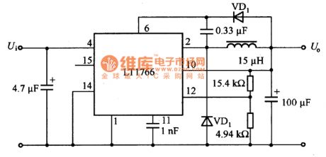
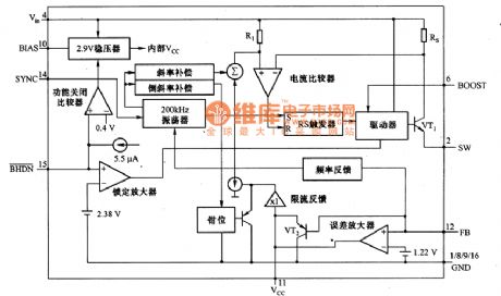
Figure a and b is the buck type converter circuit formed by the LT1766. It is a non-isolated buck type DC/DC converter with 5.5 ~ 60 V input voltage and 5 V / 1 A input. The LT1766 is a buck switch integrated regulator with all the functions that the buck type converter requires such as oscillating circuit, control circuit, switch transistor, etc. The oscillation frequency is 200 KHZ, the peak current of the on chip power transistors (VT1) is 1.5 A. (View)
View full Circuit Diagram | Comments | Reading(639)
RASTER_HORIZONTAL_SWEEP_GENERATOR
Published:2009/7/16 21:09:00 Author:Jessie

Input from 400-kc timing generator triggers Q4 through Q2 and T1,making C3 discharge to Provide sweep retrace, Negative sweep is similar except that capacitor is charged from minus 150 v.-R. P. Rufer and W.A. Karlotski, Use Raster Oscilloscopes for Faster Time Measurements,Electronics,35 52,p 38-42. (View)
View full Circuit Diagram | Comments | Reading(906)
| Pages:738/2234 At 20721722723724725726727728729730731732733734735736737738739740Under 20 |
Circuit Categories
power supply circuit
Amplifier Circuit
Basic Circuit
LED and Light Circuit
Sensor Circuit
Signal Processing
Electrical Equipment Circuit
Control Circuit
Remote Control Circuit
A/D-D/A Converter Circuit
Audio Circuit
Measuring and Test Circuit
Communication Circuit
Computer-Related Circuit
555 Circuit
Automotive Circuit
Repairing Circuit