
Circuit Diagram
Index 720
TOGGLING_TOUCH_SWITCH
Published:2009/7/13 2:45:00 Author:May

Uses half of Motorola MC14013 as flip-flop that changes state each time contacts are bridged by resistance of finger. For status display, LED driven by 2N3903 transistor can be added. Possible drawback is bouncing if finger is carelessly applied.-V. Gregory, CMOS Touch Switches-Convenient, Less $ and Sexy, EDN Magazine, May 5, 1976, p112. (View)
View full Circuit Diagram | Comments | Reading(829)
RELAY_ONLY_MVBR_FOR_A_C
Published:2009/7/16 5:22:00 Author:Jessie

Use of a-c latching relay and rectifier diodes permits operation of low-frequency relay-type mvbr from a-c source.-R. L. Ives, Multivibrator for Low Frequencies Uses Relays, Electronics, 34:32, p 166-169. (View)
View full Circuit Diagram | Comments | Reading(840)
OPEN_FUSE_DETECTOR
Published:2009/7/16 5:22:00 Author:Jessie
Magamp circuit uses bridge unbalance to operate control relay when protective fuse opens in digital com puter, to remove d-c voltages from fused section. One of 15 control windings of series-connected magnetic amplifier is placed across each fuse, with appropriate current-limiting resistor in series with each winding. (Only representative control windings are shown)-J. Maroz, Magnetic Amplifier Detects Open Fuses, Electronics, 31:29, p 86-92. (View)
View full Circuit Diagram | Comments | Reading(874)
SOS_ON_TWO_FREQUENCIES
Published:2009/7/16 5:22:00 Author:Jessie

Transistors and tubes are combined for maximum power efficiency at 5-w output. Operates on 500-kc and 8.326.Mc distress frequencies. Code-wheel-operated photoelectric flip-flop automatically switches bands and keys transmitter in SOS code.-H. B. Weisbecker, Distress Transmitter is Hybrid, Electronics, 31:31, p 98-100. (View)
View full Circuit Diagram | Comments | Reading(887)
1_LIGHT_AIRBORNE_MARKER_BEACON
Published:2009/7/16 5:20:00 Author:Jessie
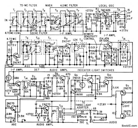
Dual-conversion 75-Mc receiver has high first i-f for good image rejection and lower second i-f for stable gain. Responds to any of three modulating frequencies (3,000 cps airways, 400-cps outer runway, and 1,300-cps middle runway).-R, G. Erdmann, Transistor Dual Conversion for Marker-Beacon Receivers, Electronics, 32:19, p 59-61. (View)
View full Circuit Diagram | Comments | Reading(1212)
MICROSEC_FALL_TIME
Published:2009/7/16 5:20:00 Author:Jessie
Fast rise time of astable mvbr is used to set and reset bistable flip-flop, whose output waveform follows that of astable with important exception that now both rise and fall limes are very fast, of the order of few microsec for 5-cps square wave.-M. I. Neidich, Astable Multi has Microsecond Fall, EEE, 11:7, p 28. (View)
View full Circuit Diagram | Comments | Reading(874)
BALANCED_PRODUCT_DETECTOR
Published:2009/7/16 5:19:00 Author:Jessie

Uses RCA CA3028A differential amplifier U1 to provide conversion gain of about 18 dB for commonly used IF values. Values of tuned circuits depend on frequency used. Unmarked resistors are on IC.-D. DeMaw, Understanding Linear ICs, QST, Feb. 1977, p 19-23. (View)
View full Circuit Diagram | Comments | Reading(1158)
THREE_STAGE_MAGNETIC_SERVO
Published:2009/7/16 5:19:00 Author:Jessie
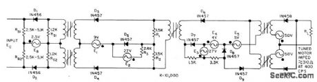
Has balanced two-core input, alternate-firing output stage, and synchronous interstage switches to eliminate interaction between stages.Power gain approaches 60 db. Zero drift is less than 0.25 deg, accuracy is within 0.5deg, and follow-up rate is 300 deg per sec.-C. C. Voice, Magnetic Amplifier Drives Gyro Indicator, Electronics, 31:7, p 114-117. (View)
View full Circuit Diagram | Comments | Reading(778)
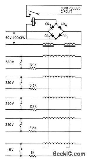
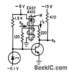
MAGNETIC_AMPLIFIER
Published:2009/7/16 5:18:00 Author:Jessie
Used in aircraft fuel low indicating system. Transistor preamp has stabilized gain of 350.-E. Van Winkle, A-C Controlled Half-Cycle Magnetic Ampli-0er, Electronics, 34:15, p 75-77. (View)
View full Circuit Diagram | Comments | Reading(1252)
MONOSTABLE_OR_CIRCUIT
Published:2009/7/16 5:16:00 Author:Jessie
Uses resistance-coupled inputs to drive tunnel diode.-F.Leary, Computers Today, Electronics, 34;17, p 64-94. (View)
View full Circuit Diagram | Comments | Reading(585)
NEON_PHOTOCONDUCTOR_INVERTER
Published:2009/7/16 5:15:00 Author:Jessie
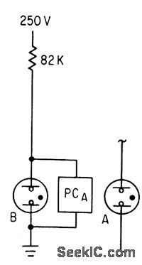
Cadmium selenide photoconductor PC and Ne2H neon lamps give low-speed inverter action for logic circuits at low cost. Neon B is on when there is no input. When neon A provides input, PC turns neon B off.-J. L. Patterson, Will Neon Photoconductors Replace Relays in Low-Speed Logic?, Electronics, 36:18, p 46-49. (View)
View full Circuit Diagram | Comments | Reading(750)
SINGLE_SUPPLY_NOP_GATE
Published:2009/7/16 5:15:00 Author:Jessie
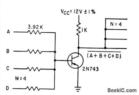
Low storage time allows medium-speed operation without turn-off base bias supply. Maximum is 1 Mc for two cascaded logic stages.-D. Hull, Using Epitaxial Transistors in Switching and R-F Circuits, Electronics, 34:13, p 52-53. (View)
View full Circuit Diagram | Comments | Reading(630)
RECEIVER_PREAMPLIFIER
Published:2009/7/13 2:45:00 Author:May
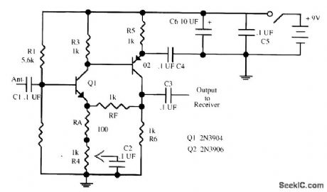
This preamplifier lets you use a short antenna over the range from 100 kHz to well over 55 MHz, with excellent sensitivity, using a vertical 30-in piece of #12 wire or a few feet of wire laying on the floor. Transistor Q1 (NPN) is directly coupled to PNP transistor Q2. Feedback from the collector of Q2 to the emitter of Q1 is accomplished by resistors RF and RA. Because of the high open-loop gain of the amplifier, the gain of the amplifier is RF/RA, or 20 dB maximum. A 1-kΩ potentiometer changes the effective value of RA resulting in a minimum gain of near unity. (View)
View full Circuit Diagram | Comments | Reading(1205)
SERIES_PNP_BASIC_LOGIC
Published:2009/7/16 5:14:00 Author:Jessie
Serves as and gale for normally open switches, and as or gate for normally closed switches. Provides phase inversion of input.-Texas Instruments Inc., Transistor Circuit Design, McGraw-Hill, NY, 1963, p 388. (View)
View full Circuit Diagram | Comments | Reading(707)
LOW_NOISE_9_MHz_AGC_CONTROLLED_AMPLIFIER
Published:2009/7/13 2:44:00 Author:May

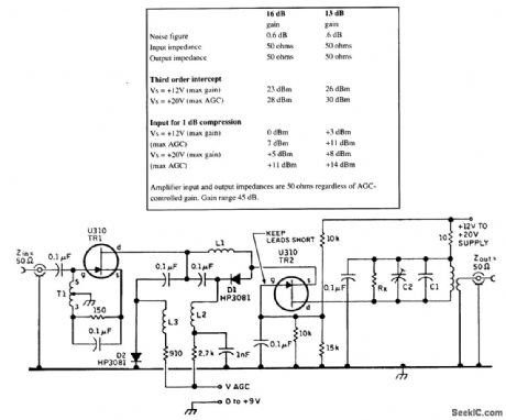
The circuit diagram of the 9-MHz amplifier is given. Note that the AGC amplifier must be capable of sinking the current through D1 at 0 V (i.e., maximum gain). The warning to keep leads short in the drain circuit of the second U310 FET arises from experience in which the initial IP3 measurements proved to be poor because of this stage's oscillating around 400 MHz.Component notes: The two U310s are Siliconix low-noise JFETs. C1 is an 82-pF ceramic, C2 is a 60-pF ceramic trimmer (Cirkit), and all other capacitors are monolithic ceramic (RS components). Resistors are l/8 Wmetalfilm (RS components). D1 and D2 are HP3081 PIN diodes (Farnell). T1 is 1518 turns of 0.224-mm diameter Bicelflux enamel on Fairite Balun core 28-43002402 (Cirkit). T2 (primary) is 2.81 μH, 31 turns of 0.314-mm Bicelflux enamel on Micrometals toroid 737-6 (Cirkit). T2 (secondary) is (1) for 16-dB gain, 3 turns, Rx 6k2; (2) for 13-dB gain, 4 turns, Rx 3k9. Note that (1) and (2) could be relay switched for use with an SSB or CW filter (loss 10 dB or 3 dB). L1, L2, and L3 have 7 turns of 9.314-mm enamel on balun core 28-43002402 (Cirkit). (View)
View full Circuit Diagram | Comments | Reading(1914)
TWO_INPUT_NIPO_NOR_GATE
Published:2009/7/16 5:13:00 Author:Jessie

Pumped tunnel diode-transistor logic gives 2-gc rate for uhf shift register using negative input-positive output gate having gain of 3 and 50.mw power drain.-Tunnel Diode-Transistor Provides Fast Logic, Electronics, 35:11, p 72. (View)
View full Circuit Diagram | Comments | Reading(667)
TWO_CELL_TO_5_V_BOOST_CONVERTER
Published:2009/7/13 2:43:00 Author:May
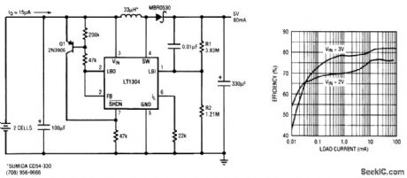
Extending the battery life of a portable device that spends most of its life time in standby mode is critical in two-cell applications. The standard LT1304 boost circuit requires two capacitors, one diode, and one inductor and provides 5 V at 200 mA from a two-cell battery with 80 percent typical efficiency. For improved efficiency at very light loads, the LT1304 switching regulator circuit shown achieves an efficiency of 50 percent at just 10 μA of load current. As indicated in the graph, high efficiency over a very wide range of load current is obtained by using the extra circuitry to control Burst Mode operation. The LT1304 is a micropower step-up dc-to-dc converter with an internal comparator that is operational in shutdown. The peak switch current limit can be set up to 1 A by the resistor at the ILIM input. In this circuit, it is set to 500 mA. The input voltage range extends down to 1.65 V, ensuring operation-even as the two-cell battery voltage drops during discharge. The on-board comparator shuts down the LT1304 micropower regulator when the output voltage is higher than the target 5-V output. In shutdown, the LT1304 consumes 10 μA of current, which is less than one-tenth of its active quiescent current of 120 μA. When the output voltage begins to droop below the target 5-V output, the comparator switches the LT1304 on again to recharge the output capacitor. (View)
View full Circuit Diagram | Comments | Reading(850)
THIN_FILM_TOGGtING_WITH_TRANSISTOR
Published:2009/7/16 5:12:00 Author:Jessie
Use of transistor stage permits cascading as for counters. Tunnel diode, which controls conducting state of transistor, is biased to have output voltages of 0.05 and 04 V. Additional film winding is needed because of phase reversal by transistor.-I. A Smay and A V. Pohm, Design of logic Circuits Using Thin Films and Tunnel Diodes, Electronics, 34;35, p 59-61. (View)
View full Circuit Diagram | Comments | Reading(700)
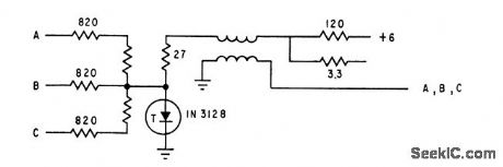
Y_AMPLIFIER_FOR_COINCIDENI_FLUX_MEM_ORY
Published:2009/7/16 5:11:00 Author:Jessie
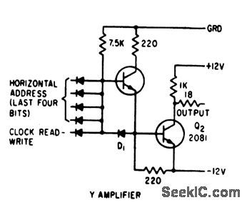
Inputs to translator section of Y amplifier are last four bits of address, which perform one out of ten translations for horizontal matrix of 1,120-bit memory.-H. F.Priebe, Jr., Three-Hole Cores for Coincident-Flux Memory, Electronics, 33;31, p 94-97. (View)
View full Circuit Diagram | Comments | Reading(803)
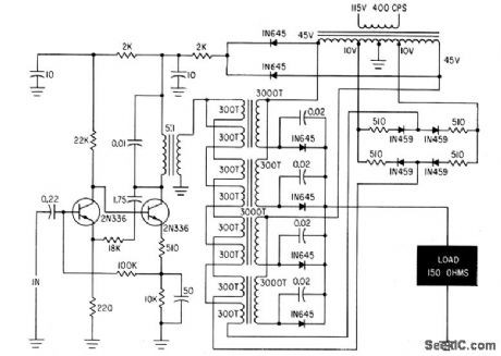
SIX_TRANSISTOFR_AM
Published:2009/7/16 5:11:00 Author:Jessie
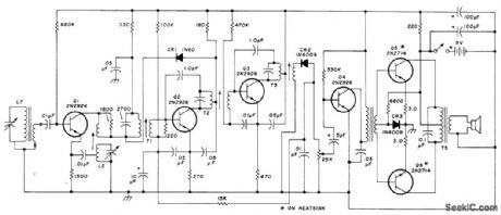
Typical older Magnavox radio uses PNP germanium transistors. L7 is loopstick antenna. Article tens how to add FET converter to radio for use as standard-frequency receiver.-H. Olson, Five-Frequency Receiver for WWV, Ham Radio, July 1976, p 36-38. (View)
View full Circuit Diagram | Comments | Reading(1349)
| Pages:720/2234 At 20701702703704705706707708709710711712713714715716717718719720Under 20 |
Circuit Categories
power supply circuit
Amplifier Circuit
Basic Circuit
LED and Light Circuit
Sensor Circuit
Signal Processing
Electrical Equipment Circuit
Control Circuit
Remote Control Circuit
A/D-D/A Converter Circuit
Audio Circuit
Measuring and Test Circuit
Communication Circuit
Computer-Related Circuit
555 Circuit
Automotive Circuit
Repairing Circuit