
Circuit Diagram
Index 711
COMPENSATED_R_C_INIEGRATOR
Published:2009/7/16 4:05:00 Author:Jessie
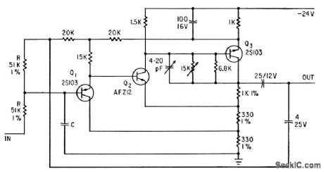
Overshoot is less than 2% at 3 db down for band-width of 20 Mc.-S. Berglund and S. Westerlund, Probes for Plasma Research with Wideband Integrators, Electronics, 35:24, p 44-45. (View)
View full Circuit Diagram | Comments | Reading(558)
INFINITE_INPUT_RESISTANCE
Published:2009/7/13 3:53:00 Author:May

Uses metal oxide semiconductor field effect transistor as buffer to give input impedance of 1015 ohms.Amplifer gain is unity within 0.1% for 100K load. When adjusted, output equals input within 10 my over allowable range of 10 v above or below ground.-A. D. Delagrange, Amplifier Provides 1015-Ohm Input Resistance, Electronics, 39:17, p 99. (View)
View full Circuit Diagram | Comments | Reading(682)
COMPUTER_FOR_SIX_BIT_BINARY_OUTPUT
Published:2009/7/16 4:04:00 Author:Jessie
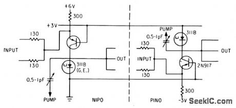
Pumped tunnel-diode-transistor logic at 300 Mc converts outputs of converter subchannels into time series of six bits. In nipo element, one or more negative pulses at input in.hibits positive-going pulse at output; other element operates at opposite half-cycles at pump source and gives opposite action.-H. R. Schindler, Semiconductor Circuits in c UHF Digital Converter, Electronics, 36:35, p 37-40. (View)
View full Circuit Diagram | Comments | Reading(672)
BASIC_VACUUM_TUBE_REGENERATIVE_DETECTOR
Published:2009/7/13 3:52:00 Author:May
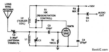
The traditional tube-based regenerative receiver is essentially an Armstrong RF oscillator with variable feedback that is connected to an antenna and a resonant circuit. C1 is usually a 140-pF variable capacitor, and L1 and L2 are wound on a plug-in coil form, with L2 typically having 10 to 20 percent of the turns on L1 and wound next to the cold side of L1. The inductance depends on the desired frequency range, but 150 kHz to about 18 MHz is typical for this circuit. (View)
View full Circuit Diagram | Comments | Reading(1622)
XENON_STROBE
Published:2009/7/13 3:52:00 Author:May

Two- transistor oscillator generates pulses at about 500 Hz for step-up by 300-mA filament transformer T1 (Radio Shack 273-1384) to charge storage capacitors C2 and C3, which are 250-V electrolytics. Simultaneously, C4 is charged through R2. After allowing sufficient time for capacitors to charge,S1 is pressed to discharge C4 through 272-1146 flashtube trigger transformer T2, which steps up voltage pulse to about 4000 V for ionizing gas in 272-1145 xenon flashtube FT1. C2 and C3 now discharge through ionized gas to produce brilliant flash of white light lasting only a few microseconds, as required for photography of objects moving at high speed. Circuit may require two cells in series for reliable operation.-F. M.Mims, Transistor Projects, Vol. 3, Radio Shack, Fort Worth, TX, 1975, p 49-60. (View)
View full Circuit Diagram | Comments | Reading(3065)
UNDERCOVER_SCANNER_ANTENNA
Published:2009/7/13 3:51:00 Author:May

The figure shows the schematic for the antenna circuit. Because the circuit is passive.no power supply is needed. Plug PL1 connects to the audio output or earphone jack of a scanner. The audio signal is then fed to J2, the earphone/antenna jack of the circuit. A 0.1-μF capacitor, C1, connects the center ( hot ) terminal of J2 to a BNC jack, J1. When an earphone is plugged into J2, C1 feeds RE from the earphone wire to the front end of the scanner, through J1, without directly connecting the audio circuit to the receiver. An earphone connected to J2 will therefore both provide audio and act as anantenna.
(View)
View full Circuit Diagram | Comments | Reading(856)
FULL_WAVE_TD_SCR_CONTROL
Published:2009/7/13 3:51:00 Author:May

Use of funnel diode between gate and cathode of each scr improves control performance of scr, to give triggering rcmge of 10° to 175°. Input sensor Rh may be photocell or any other resistive fransducer.-TD/SCR Combos for Sale, EEE, 12;3, p62-64. (View)
View full Circuit Diagram | Comments | Reading(609)
QUADRATURE_DETECTOR_DESIGN
Published:2009/7/13 3:51:00 Author:May
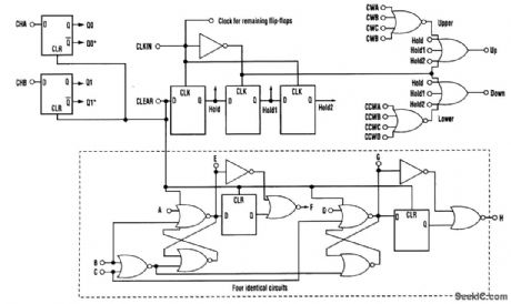
One common electrical requirement when dealing with motion control is to monitor the angular position of a rotating object.Quite often, an optical encoder is attached to a rotating shaft, and the encoder's quadrature outputs provide angular displacement information. The key is to turn those quadrature signals into clock pulses, and then into a displacement count that's useful for your application. This circuit requires a reset as well as a clock for sampling the input data. The clock frequency needs to be adjusted to guarantee at least one rising clock edge for each input state change. The circuit takes a set of quadrature signals (CHA, CHB), samples them with CLKIN, and generates output clock pulses (UP or DN) for each input state change. The up/down output clock pulses then can be fed directly into 74XX193 counters as the up and down clocks. If CLKIN is synchronized to external timing, the 193 ripple counter's output can be latched out of phase with the updates to ensure stable counter values. The timing diagram shows the internal functionality of the design. Intervals 1 to 5 illustrate the reset function, which blanks startup instability conditions.Intervals 5 through 12 show timing for a jitter pulse that's been sampled. Interval13 depicts a jitter pulse that missed being sampled and, therefore, caused no change in the output. The remaining intervals illustrate complete cycles for each direction of motion. (View)
View full Circuit Diagram | Comments | Reading(2395)
BENCH_POWER_SUPPLY_METER
Published:2009/7/16 4:04:00 Author:Jessie

The heart of the digital meter is the Harris ICL7107 A/D converter. The 7107 contains all the active devices needed to construct the voltmeter. These include the segment decoders and LED display drivers. The optional push-button switch connected to pin 37 of the ICL7107 permits the display to be tested. When that pin is connected to +5 V, the display will indicate -1888, testing all the segments. If a liquid-crystal display is preferred, substitute an ICL7106CPL for the 7107. All pin connections will be the same, except that pin 21 will become the backplane instead of the digital ground. (View)
View full Circuit Diagram | Comments | Reading(7482)
40_m_LOOP_ANTENNA
Published:2009/7/13 3:50:00 Author:May

A cliff-dweller's dream, this 40-m loop can get apartment-based hams on the air. It also makes a great receiving antenna. The matching transformer, T1, is wound on T50-2 toroid core. The primary consists of 4 turns of 18-gauge enameled copper wire, and the secondary consists of 12 turns of 20-gauge enameled copper wire. Close-wind the secondary and the primary, and make sure that the two windings do not overlap. (View)
View full Circuit Diagram | Comments | Reading(2320)
GATEDBEAM_SQUAREWAVE_GENERATOR
Published:2009/7/16 4:04:00 Author:Jessie
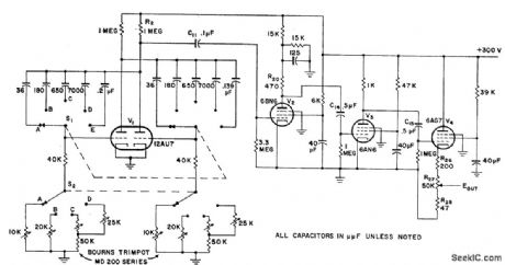
Amplifies without attenuation up to tenth harmonic of square-wave fundamental, from which output of 50 to 500,000 pps can be adjusted over desirable range without wave form distortion. Uses twin-triode 12AU7 as symmetrical mvbr, 6BN6 as gated-beam tube, 6AN6 as wideband amplifier, and 6AG7 as cathode-follower output. Operating frequencies are changed by S1 and S2. R27 adjusts output signal level from 0.8 to 8 v peak to peak. Rise time for 500-kc signal is better than 0.07 microsec. Provides 5 distinct repetition rates (50, 1,000, l0,000,100,000, and 500,000 pps) for checking amplifiers up to at least tenth harmonic of fundamental repetition ratio.-Gated-Beam Tube Square-Wave Generator, Electronic Circuit Design Handbook, Mactier Pub. Corp., N.Y., 1965, p 175. (View)
View full Circuit Diagram | Comments | Reading(2145)
12_LED_SEQUENTIAL_DRIVER
Published:2009/7/13 3:49:00 Author:May

A demultiplexer selects a different LED for each binary number at its input. The counter resets after a count of 12. (View)
View full Circuit Diagram | Comments | Reading(622)
TIMER_SWITCH_OFF_FOR_ENLARGER
Published:2009/7/13 3:46:00 Author:May
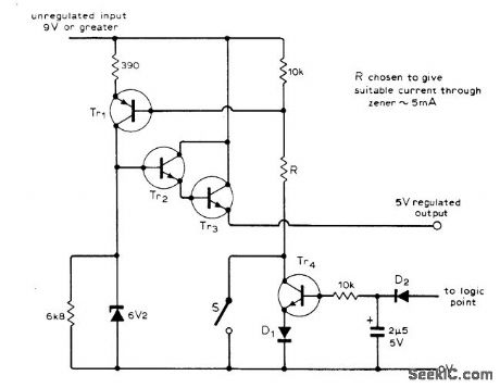
Circuit shows power supply designed to operate digital exposure timer using TTL. Since timer logic is needed only when enlarger lamp is on, power supply circuit will be turned off automatically when timer goes low and turns off enlarger lamp at end of exposure, Switch S is closed when timer cycleis activated, setting timer out-put at 5 V and turning on lamp. Transistor and diode types are not critical, Since D2 is con-netted to logic point of timer, power supply re-mains on when S is released, until completion of timer cycle.-E. R. Rumbo, Automatic Switch-Off Power Supply, WI'reless World, Feb.1976, p 77. (View)
View full Circuit Diagram | Comments | Reading(751)
PLL_LOCK_DETECTOR
Published:2009/7/13 3:46:00 Author:May

When the loop is locked, the waveforms at pins 1 and 2 of CD4046B are almost identical, differing only in polarity. This holds the output of the NOR gate low. When the loop is not locked, the output of the NOR gate is a series of pulses. This charges the 0.047-μF capacitor, and causes a low output from the CMOS buffer. (View)
View full Circuit Diagram | Comments | Reading(1047)
R_C_SERVO_DRIVER_CIRCUIT
Published:2009/7/13 3:46:00 Author:May
The circuit shown produces the necessary pulse signal to drive R/C servos through a 90°range by adjustment of the pot R2. (View)
View full Circuit Diagram | Comments | Reading(844)
450_MC_R_F_FOR_AERONAUTICAL_BAND
Published:2009/7/13 3:46:00 Author:May
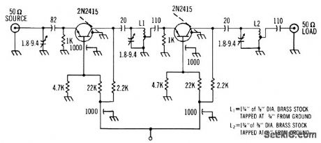
Common-base configuration gives slightlymore power gain at this frequency that common-emitter circuit,Power gain is 20 db,noise figure 4.5 db, and bandwidth 10 Mc,-Texas instruments Inc., sond-State Communications,McGraw-Hill, N,Y., 1966, P 298. (View)
View full Circuit Diagram | Comments | Reading(605)
HV_STATIC_DETECTOR
Published:2009/7/13 3:45:00 Author:May

One leg of a Wheatstone bridge is replaced by an MPF102 N-channel JFET. The JFET's high gate input impedance turns the simple bridge circuit into a very sensitive high-voltage static detector.The JFET's gate is tied to ground through four 22-MΩ resistors. A 1- to 2-in piece of solid-copper wire is connected directly to the JFET's gate and serves as the input sensor. With the sensor clear, adjust R8 for a zero meter reading. Run a comb through your hair and move it toward the sensor.The meter should go off the scale. Place the staticsensor next to your computer or any static sensitive equipment and take special notice when the meter moves. (View)
View full Circuit Diagram | Comments | Reading(2231)
60_MC_AMPLIFIER
Published:2009/7/13 3:44:00 Author:May
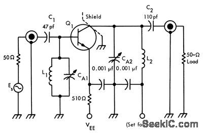
Design equations are given and example worked out for 10-Mc band-width at 60 Mc and gain of 11.5 db, using 2N743. L1 is 1.5 turns of No. 14 wire and L2 is 2 turns, both 0.25 inch in dicmeler. VEE is 5 v.-Texas Instruments Inc., Solid.State Communications, McGraw-Hill, N.Y., 1966, p 87. (View)
View full Circuit Diagram | Comments | Reading(605)
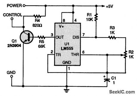
MISSING_PULSE_DETECTOR
Published:2009/7/13 3:44:00 Author:May

A missing-pulse detector is a circuit whose output is triggered only when there is a loss of signal at its input. In the circuit shown, the 555 timer IC is configured as a one-shot multivibrator that produces a pulse whose width is determined by the value of resistance R and capacitance C, shown in the schematic. The values for those parts can be calculated by using the formula T=1.1RC. Select values that make the output pulses about twice as wide as the input trigger pulses from the control line. As long as there is a steady stream of input trigger pulses, the 555 will output a logic high. If there is only one input pulse period, the 555 will time out and its output will go logic low until the next trigger pulse arrives. The logic low at the 555 output can trigger an alarm, a time recorder, a counter, or any other device. (View)
View full Circuit Diagram | Comments | Reading(0)
195_V_FROM_27_V_BATTERY
Published:2009/7/13 3:43:00 Author:May

Used to provide precise voltage levels required by portable trigger unit designed to fire up to five different flash units at equal intervals that may range from 11 ms to 11 s. Article gives all circuits.-R. Lewis, Multi-Flash Trigger Unit, Wireless World, Nov.1973, p 529-532.
(View)
View full Circuit Diagram | Comments | Reading(931)
| Pages:711/2234 At 20701702703704705706707708709710711712713714715716717718719720Under 20 |
Circuit Categories
power supply circuit
Amplifier Circuit
Basic Circuit
LED and Light Circuit
Sensor Circuit
Signal Processing
Electrical Equipment Circuit
Control Circuit
Remote Control Circuit
A/D-D/A Converter Circuit
Audio Circuit
Measuring and Test Circuit
Communication Circuit
Computer-Related Circuit
555 Circuit
Automotive Circuit
Repairing Circuit