
Circuit Diagram
Index 718
BIKE_SPEEDOMETER_CIRCUIT
Published:2009/7/16 5:39:00 Author:Jessie

The proximity detector senses the passing of the PC board pieces as the wheel rotates, providing an output signal, which has a clean transition between high and low voltage levels, and is ideal for triggering counting or processing circuits. Next is the frequency-to-voltage converter, and, because a reasonable degree of accuracy is required, the LM2917N-8 IC has been chosen. The output from this IC is fed to two bar-graph ICs, which drive a 20-LED display. (View)
View full Circuit Diagram | Comments | Reading(4478)
FULL_WAVE_SYNCHRONOUS_BECTIFIER
Published:2009/7/13 2:52:00 Author:May
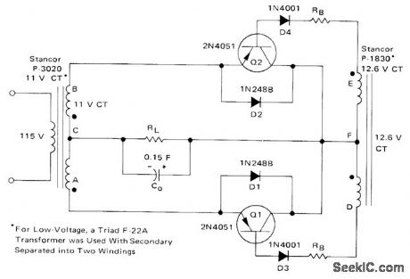
Transistors are biased on alternately by AC input voltage, to supply load current on alternate half-cycles. Silicon diodes D1 and D2 protect transistors from charging current of capacitive load when circuit is turned on, Capacitor discharge problems are minimized by use of diodes D3 and D4 in base circuits of transistors.-B. C. Shiner, Improving the Effilciency of Low Voltage, High-Current Rectification, Motorola, Phoenix, AZ, 1973, AN-517, p 4. (View)
View full Circuit Diagram | Comments | Reading(811)
OPTOELECTRONIC_BRIDGE_ELEMENT
Published:2009/7/16 5:39:00 Author:Jessie

Lamp With rheostat varies resistance of photocell over range of 10,000 ohms to give stable nonreactive resistance element for r-f bridge. –R.H. Wagner, Variable R-F Resistor Attained With Photocell, Electronics, 37:26, p 67. (View)
View full Circuit Diagram | Comments | Reading(636)
20_CHANNEL_DECODER_FOR_AUDIO_TONES
Published:2009/7/13 2:51:00 Author:May


L-C filter in each decoder is tuned to channel tone,with 35-db adjacent-channel rejection.Rectified output of detector D1 drives two-stage d.c amplifier having relay load. Used in Mercury spacecraft command receiver.-R.Elliott,First Details on Mercury Spacecraft Command Receiver,Electronics,36:5,p32-35 (View)
View full Circuit Diagram | Comments | Reading(793)
CASCODE_ADDER
Published:2009/7/16 5:37:00 Author:Jessie

Gives gain of 600 when used as null detector of 400-cps impedance bridge, with measuring accuracy of one part per million.-W. A. Rhinehart and L. Mourlam, FET Performs Well in Balancing Act, Electronics, 38:19, p 88-92. (View)
View full Circuit Diagram | Comments | Reading(744)
TOGGLE_SWITCH
Published:2009/7/13 2:49:00 Author:May

Touching one 0.5-inch-square copperclad pattern on printed-circuit board turns switch circuit on by giving high out-put. Touching other plate turns switch off. LED between output and ground shows status of switch. For proper switching, circuit must con nect to line-operated DC power supply.-R. D. Wood, Replace Bulky Mechanical Switches with Touch Controls, EDN Magazine, April20, 1978, p 132-133. (View)
View full Circuit Diagram | Comments | Reading(985)
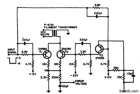
RIPPLE_ADDER
Published:2009/7/16 5:36:00 Author:Jessie

When a device under test needs a dc voltage applied with ripple superimposed, this circuit can handle the task. The power supply for the +V input will need to be set about 20 percent higher than the desired output. The supply should be well regulated, because it directly affects the output volt-age. A function generator set to the desired waveform, amplitude, and frequency must be connected to the ripple input. Because of resistor tolerances, the final voltage adjustments will have to be made by monitoring the output. U2 will drive capacitive loads as long as the dc + peak ac doesn't exceed 200 mA. The frequency response of the ripple adder with a 5-V p-p output ranges from dc to past 100 kHz. R5 and C3 should be located as close as possible to U2. R1 can be altered to change the ratio between the input and output voltages. (View)
View full Circuit Diagram | Comments | Reading(818)
DIODE_SAMPLING_BRIDGE
Published:2009/7/16 5:36:00 Author:Jessie
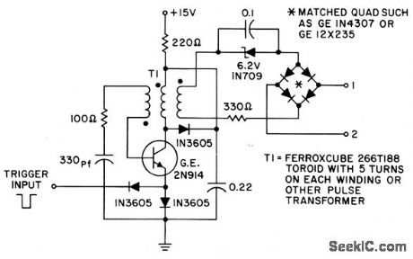
Uses diode matched quad with blocking-oscillator driving circuit. Negative input pulse triggers oscillator, generating pulse about 100 nsec wide, to forward-bias bridge diodes and reduce impedance between terminals 1 and 2 to about 5 ohms. Between pulses, diodes are reverse biased by capacitor charge and impedance between terminals rises to 1,000 meg.- Transistor Manual, Seventh Edition, General Electric Co., 1964, p 450. (View)
View full Circuit Diagram | Comments | Reading(2166)
FET_MIXER
Published:2009/7/16 5:36:00 Author:Jessie

Double-balanced mixer developed for use in high-quality high-fidelity communication receiver has high input impedance (about 1000 ohms). Two-tone 176-mV signal produces third-order intermodulation distortion 68 dB down.-U. L. Rohde, Optimum Design for High-Frequency Communications Receivers, Ham Radio, Oct. 1976, p 10-25. (View)
View full Circuit Diagram | Comments | Reading(1615)
JAMMIX_STEREO_MIXER
Published:2009/7/16 5:35:00 Author:Jessie

Here is the schematic diagram for JamMix. Note that nine out of ten sections from five MC1458C dual op amps are used. The INSTRUMENT jack, J1, provides a signal to IC1-a, which is a noninvert-ing buffer amplifier with a gain of 2. The gain is determined by R3 and R4. The amplified instrument signal is fed to audio-gain stage IC1-b, which is controlled by potentiometer R6. The circuit location of control R6 provides a desirable interplay with volume control on the guitar. Whenever the output of IC1-b exceeds about 2V p-p, light-emitting diodes LED1 and LED2 begin to illuminate and clip the audio signal, providing a high-quality distortion effect. The LEVEL control, RIO, sets the level of the output of the high-gain distortion stage IC4-a, which, in turn, drives the ganged potentiometers (R14a and R14b). Unity-gain amplifiers IC5-a and IC5-b feed summing amplifiers IC2-b and IC3-b, which in turn drive the external load connected to stereo OUT jack J3. The load can be either stereo headphones or additional external stages used for audio amplification. Integrated-circuit sections IC2-a and IC3-a are noninverting amplifiers, each with a gain of 2. Their inputs are the line-level stereo input signals, each having a gain of 2. Their outputs mix with the instrument signal in ampli-fiers IC2-b and IC3-b; both of these amplifiers also have a gain of 2. (View)
View full Circuit Diagram | Comments | Reading(925)
PULSED_OSCILLATOR
Published:2009/7/16 5:35:00 Author:Jessie


Circuit is pulsed on only when required ,as in tone generators where output is needed only occasionally and power must be conserved. Uses Wien-bridge oscillator have rang of 100 cps to 100 kc, which operates only when gating pulse is applied to input. Amplitude of output oscillations varies with amplitude of gating pulsed.-R.C. Lavigne and L. L. Kleinberg, Pulsed Oscillator Conserves Power, Electronics, 39:17, p 98-99. (View)
View full Circuit Diagram | Comments | Reading(1063)
DIFFERENTIAL_BOOTSTRAP_AMPLIFIER_WITH_BRIDGE_FEEDBACK
Published:2009/7/16 5:35:00 Author:Jessie

Uses bridge feedback to give bandwidth of 30 to 300 kc with 40 db gain, for handling group of telephone channels as baseband amplifier.-N. A. Zellmer, Getting the Most Out of Feedback, Electronics, 39:2, p 66-72. (View)
View full Circuit Diagram | Comments | Reading(703)
DRAIN_COUPLED_ADDER
Published:2009/7/16 5:34:00 Author:Jessie

Gives gain of 1,400 for null detector of 400-cps impedance bridge, with measuring accuracy of one part per million.-W. A. Rhinehart and L.Mourlam, FET Performs Well in Balancing Act, Electronics, 38:19, p 88-92. (View)
View full Circuit Diagram | Comments | Reading(747)
PHASE_DIFFERENCE_BRIDGE
Published:2009/7/16 5:33:00 Author:Jessie
Develops d-c error voltage proportional to phase difference between two applied signals, one of which is 60-cps line-frequency reference. Can also correct oscillator outputs and serve as pulse-width discriminator.-D. P. Dorsey, Transistor Bridge Detector, EEE, 13:1, p 75. (View)
View full Circuit Diagram | Comments | Reading(753)
PULSE_HEIGHT_DETECTOR
Published:2009/7/16 5:31:00 Author:Jessie

Photodiode held against screen of scope unbalances bridge when illuminated by pulse on screen. Bridge output can control another scope for displaying and measuring pulses whose amplitude and period vary randomly.-I. Baird, Pulse Frequency Measured by Photoconductor and Scopes, Electronics, 38:13, p 77. (View)
View full Circuit Diagram | Comments | Reading(895)
MULTI_WAVEFORM_OSCILLATOR
Published:2009/7/16 5:31:00 Author:Jessie

By varying collector load, emitter resistors, and C, oscillator can produce triangular wave, square wave up to 30 Mc, microwattt audio signal, or serve as voltage-controlled oscillator. Values shown, with 6.v supply and 0.01 mfd mined for C, give 0.8 V peak-to-peak square wave at about 1 Mc. –P. Lefferts, Multi-Oscillator Gives Simple Waveforms, 30-Mc Output, EEE, 12:10, P 60. (View)
View full Circuit Diagram | Comments | Reading(980)
SIGNAL_POWERED_TRANSPONDER
Published:2009/7/16 5:30:00 Author:Jessie

Power received at frequency of tuned antenna circuit energizes crystal transistor stage, to make it oscillate at a different frequency. Can be used in aircraft or vehicle to make it radiate position-determining signal when interrogated by powerful transmitter at base station. –L. R. Crump, Radio Waves Power Transistor Circuits, Electronics, 31:19, p 63-65. (View)
View full Circuit Diagram | Comments | Reading(1102)
GATED_DIODE_BEACON_MODULATOR
Published:2009/7/16 5:30:00 Author:Jessie

Replaces hydrogen-thyratron line-pulsing modulators formerly used to plate-pulse pencil triode in beacon transmitter. Maximum pulse rate is 5,000 pps. -W. H. Lob, Solid-State Pulse Modulator, Electronics, 33:30, p 72-74. (View)
View full Circuit Diagram | Comments | Reading(711)
SCS_SQUARE_WAVE_GENERATOR
Published:2009/7/16 5:30:00 Author:Jessie

R1-C determines half the period, and R2-C the remainder. R1 should equal R2 for square wave output. Potenliometer varies pulse width without affecting frequency. Outputs are equal and oppositely phased.- Transistor Manual, Seventh Edition, General Electric Co., 1964, p 434. (View)
View full Circuit Diagram | Comments | Reading(635)
CRASH_RESISTANT_BEACON
Published:2009/7/16 5:29:00 Author:Jessie

Designed to withstand shocks up to 1,100 g and extreme environments, 5.7-1b beacon is thrown free of crashing aircraft and automatically starts transmitting pulse-modulated 243-Mc distress signal. -D. M. Makow, Radio Beacon Helps Locate Aircraft Crashes, Electronics, 33;4, p 54-56. (View)
View full Circuit Diagram | Comments | Reading(729)
| Pages:718/2234 At 20701702703704705706707708709710711712713714715716717718719720Under 20 |
Circuit Categories
power supply circuit
Amplifier Circuit
Basic Circuit
LED and Light Circuit
Sensor Circuit
Signal Processing
Electrical Equipment Circuit
Control Circuit
Remote Control Circuit
A/D-D/A Converter Circuit
Audio Circuit
Measuring and Test Circuit
Communication Circuit
Computer-Related Circuit
555 Circuit
Automotive Circuit
Repairing Circuit