
Circuit Diagram
Index 719
STRIP_CHART_RECORDER_FROM_OLD_COMPUTER_PRINTER
Published:2009/7/16 5:29:00 Author:Jessie

Converting an obsolete computer printer into a strip-chart recorder is both easy and inexpensive. The chart recorder works by comparing the voltage on a potentiometer to the voltage on a temperature-sensing thermistor. The potentiometer is mechanically connected to the printer carriage. A marking pen is also connected to the printer carriage. Any difference in the voltages on the potentiometer and the temperature sensor causes an op amp to attempt to bring the voltages back into balance. In the course of this, the print-head carriage is moved left or right, thereby causing a mark on the paper. A standard 741 op amp is used as a comparator. The comparator monitors the voltages at the junctions, marked TP1 and TP2. The op amp compares the voltages from the two networks at its inputs (pins 2 and 3). When the voltages are identical, the op amp's output (pin 6) is zero, so neither driver transistor (Q1 and Q2) turns on; therefore, the motor does not turn. But if thermistor R2's resistance changes because of a change in air temperature, a new voltage occurs at the op amp's inverting input (pin 2). For example, assume that R2 decreases.
The pin 2 voltage then increases, so the op amp's output swings negative, thereby biasing Q2 on. That in turn starts the motor, which moves the carriage left or right. Potentiometer R5 is also coupled to the carriage, so, as the carriage moves, R5's wiper moves, thereby varying the voltage on the noninverting input of IC1. When the op amp's input voltages become equal, the output goes to zero, both transistors turn off, and so does the motor. Now the circuit remains quiescent until the temperature changes again. (View)
View full Circuit Diagram | Comments | Reading(2375)
Steam iron automatic protection circuit diagram
Published:2011/8/4 5:08:00 Author:Rebekka | Keyword: Steam iron, automatic protection

The circuit is shown as above, the commercial power passes C5, R7, R8 buck, VD7 ~ VDl0 commutating and VD11 regulator. The circuit provides operating voltage. When the iron is put horizontally, the mercury switch S downward about 15o and in a disconnected state. At this time, IC1-a outputs low level, C1 is charged by R2, ICl-c outputs low level, ICl-d has outputs low, VD3, VD4, IC1-e form NAND gate output high level, VT2 is turned on, relay Jl pulls in, then heating wire is heating, H neon lights are lit. (View)
View full Circuit Diagram | Comments | Reading(3580)
BASIC_HARTLEY
Published:2009/7/16 5:28:00 Author:Jessie

Sine-wave oscillator, tunable over 3:1 frequency range by C4, uses switching transistor. Used in pulse generator for testing high-speed digital computers.-L. Neumann, Transistorized Generator for Pulse Circuit Design, Electronics, 32:14, p 47-49. (View)
View full Circuit Diagram | Comments | Reading(751)
35_4_MHz_WITH_TUNING_DIODES
Published:2009/7/16 5:28:00 Author:Jessie

Miniaturized communication receiver was developed for use as tunable IF fed by external converter for all-band coverage up to 30 MHz, Motorola MVAM-1 triple tuning diode serves in place of customary three-gang tuning capacitor. Two Murata SFD-455D ceramic filters provide IF selectivity. MFC6030 voltage regulator provides around 7 VDC with regulation required for diode tuning. Regulator also supplies VFO and BFO. Standard 3/8-in diameter 455-kHz transistor IF transformers were stripped and used for coil forms. T3 is 455-kHz IF with secondary changed to 1 turn. Remove pins 4, 6, and 8 from Silicon General SG3402T mixer.-R. Megirian, Design Ideas for Miniature Communications Receivers, Ham Radio, April 1976, p 18-25. (View)
View full Circuit Diagram | Comments | Reading(1950)
Light Control Cockcrow Ciruit
Published:2011/8/4 2:42:00 Author:May | Keyword: light control, cockcrow
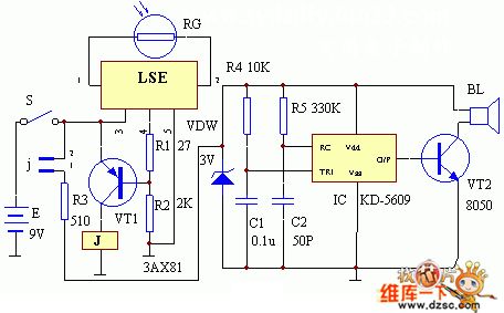
The circuit working principle of this set is shown in the diagram. At night, when there is no light shining on the photoresistor RG, the essential resistance of RG is very large, (larger than 50K) , so LSE's pin ①, ② is equal to open, LSE's pin ④ outputs low level, triode VT1 is break over, relay J excitation actuation, its normal close point j is opened, analog cockcrow circuit IC KD5609has no power and does not work. When daybreak, there is light shine on RG, the essential resistance of RG changeslower ( <50k) , at this moment , LSE' pin ④ outputs high level, triode VT1 is closed, relay J is released, its normal close point j is closed, analog cockcrow circuit is electrified and worked, andit sends clearly crow from the indicator speaker BL.
(View)
View full Circuit Diagram | Comments | Reading(807)
LINEAR_TECHNOLOGY_POWER_SOLUTIONS
Published:2009/7/13 2:49:00 Author:May

An increasing number of portable devices need 5-V-to-3.3-V converters. High efficiency at up to 1 A is needed to power 3.3-V ICs, such as power-hungry high-speed microprocessors. The LTC1265-3.3 high-efficiency switching regulator circuit shown generates up to 1 A at 3.3 V. The LTC1265-3.3 utilizes a constant OFF-time current-mode architecture for excellent line and load regulation and contains an internal P-channel power MOSFET with 0.3 Ω ON resistance, as well as a low-battery detector. The output current is user-programmable by selection of the current sense resistor Rsense according to the formula Iout = 100 mV /Rsense. Short-circuit protection is inherent in the current-iiiode architecture and limits the maximum current. The LTC1265 draws only 160 μA quiescent current under no load and just 5 μA when placed in shutdown. (View)
View full Circuit Diagram | Comments | Reading(928)
3_LIGHT_MARKER_BEACON_ADAPTER
Published:2009/7/16 5:27:00 Author:Jessie
Separates the three marker beacon modulating frequencies and converts them to voltages for operating three color-coded lights in air-craft. When added to one-light receiver, adapter requires only two more electronic switches, in addition to loss amplifier and filters.-R. G. Erdmann, Transistor Dual Conversion for Marker-Beacon Receivers, Electronics, 32:19, p 59-61. (View)
View full Circuit Diagram | Comments | Reading(1054)
FREQUENCY_RESPONSE_TESTER
Published:2009/7/16 5:26:00 Author:Jessie

The two quad op-amp sections, U3-c and U3-d, are configured as a linear ramp generator. With switch S2 in the SWEEP position, as shown, the output of U3-d is low. Zener diodes D2 and D3 limit that output to about -7V, which is the 6.2-V reverse drop across D3 plus the forward drop of D2. The internal short-circuit protection of the op amp limits the zener current to several milliamperes. Because the output of U3-d is negative, integrator U3-c generates a linear ramp in a positive direction, at a rate determined by the resistance of R4 and R29 and the capacitance of C5. A portion of that output is fed back to the noninverting input of U3-d. Because U3-d is basically operating as a comparator with its inverting input grounded, its output will switch positive as soon as its noninverting input crosses zero volts. The overall effect is to produce a saw tooth waveform with an amplitude of over 10-V p-p. That is more than sufficient for just about any scope's horizontal input. Next, the linear ramp under-goes a series of level and offset adjustments via resistors R7, R8, R9, R22, and R23, and is then applied to the base of Q1. The emitter-coupled transistors, Q1 and Q2, in combination with U3-b, produce an antilog transfer function. The output at the collector of Q2 will be logarithmic with respect to the in-put, yielding a one-decade voltage differential for every few volts of input. Next, U4-a inverts the polarity of the signal, so that it starts high and ends low. That is necessary because the output frequency of the 8038 function generator, U5, is inversely proportionalto its input voltage. The ICL8038 function generator produces constant-amplitude sine waves, as well as triangle- and square-wave outputs, from 20 Hz through 20 kHz. Also, its output frequency is nearly a perfect inverse proportional to its in-put voltage, so driving its input with a logarithmic sweep circuit will produce the balanced, three-decade frequency sweep. The sine-wave output from U5 is fed to the voltage divider made up of R18 and R19, which restores the dc offset to zero. The voltage-divider output is then applied to potentiometer R28 for output-level control, and is subsequently routed to U4-b for a boost in both amplitude- and current-drive capability. The output can range from 0 to over 10 V p-p. (View)
View full Circuit Diagram | Comments | Reading(3853)
RF_PREAMP_SUPPLY
Published:2009/7/13 2:49:00 Author:May

Early tube-type receivers used filament voltages of 6.3 and 12.6 Vac, but had no low-voltage dc power supplies. The figures show how to borrow a little of the filament voltage, which is rectified and regulated to provide 12 Vdc for the preamp. In the 6.3-Vac version, diodes D2 and D3 act as a simple voltage doubler to step the input voltage up to approximately 15 Vdc. While the 220-μF capacitors used for the voltage doubler are sufficient for the load presented by the preamp, they will not provide the 115 V dc to the input of the regulator at more than about a 25-mA load. If other circuits will be used with these dc power sources, then the 220-μF capacitors should be increased ac-cordingly (2200 μF will provide about 65 mA regulated output). (View)
View full Circuit Diagram | Comments | Reading(868)
High voltage speed optocoupler and application circuit diagram
Published:2011/8/4 5:03:00 Author:Rebekka | Keyword: High voltage speed optocoupler , application circuit
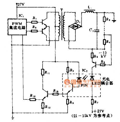
High speed optocouplers, its technical parameters are as follows: Rise time t1 ≤ 300ns; Circuit eye transfer ratio CTR = 50%; Isolation voltage VSO ≥ 15000V; Output transistor reverse breakdown voltage V (BR) CEO ≥ 50V.
The optical coupler can be widely used for the high-voltage isolators, high-voltage pulse transformers and high-voltage power circuit voltage stability control system. The control systems is used for high voltage regulator circuit. The fast high-voltage electrical coupling in this circuit play two roles. First one is to achieve the output voltage feedback loop in the input circuit and high voltage isolation between the low-voltage circuits; The other role is to achieve high output voltage feedback signal.
Note: The high pressure side +27 V DC power supply is independent, but its pressure level must be greater than 15KV. (View)
View full Circuit Diagram | Comments | Reading(2526)
ADJUSTABLE_ODDS_LORRERY
Published:2009/7/13 2:48:00 Author:May
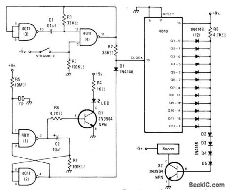
Odds for lottery are set by diode matrix connected to output of 4040 counter. Range is from 1 :2 to 1 : 1024. To use, close scramble switch for a second or two to make free-running oscillator drive counter at high rate, then let contestant hit toueh plate to trigger flip-flop that advances counter one step. If counter was frozen at next to last connected diode, next diode is biased off and Q2 energizes buzzer. For 50-50 odds, connect only diode at output Q1. For odds of 1 in 10, connect diodes only to outputs Q2and Q4 for binary 1010 or 10. With all diodes connected as shown, odds are 1:1024.-J. Sandier, Play 'Random Chance,' Modern Electronics, Oct. 1978, p 42-43 and 88. (View)
View full Circuit Diagram | Comments | Reading(2309)
RZ_TO_NRZ_ONE_SHOT
Published:2009/7/16 5:26:00 Author:Jessie
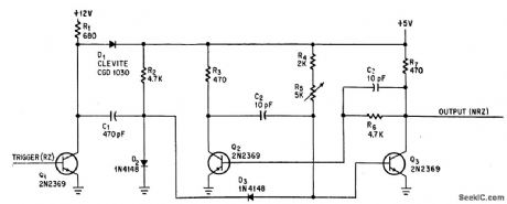
Zero recovery time of monostable multivibrator arrangement, achieved by using energy of input capacitor to recharge timing capacitor C2, makes circuit useful for converting digital data from return-to-zero format to non-return-to-zero. -P. T. Rux, One-Shot Multivibrator with Zero Recovery Time, Electronics, 39:2, p 75-76. (View)
View full Circuit Diagram | Comments | Reading(954)
DEBOUNCE_FOR_TOUCH_SWITCH
Published:2009/7/13 2:47:00 Author:May

Two CMOS inverters respond to high-impedance path between electrodes of touch switeh to provide finger-touch sensitivity and positive switching action with minimum components. Large time constant of R1C1 requires wait of about 4 s before attempting to retrigger circuit. C2 prevents oscillation from 60-Hz pickup when electrodes are touched.-H. Manell, CMOS lnverters Implement Finger-Touch ON-OFF, EDN Magazine, Jan. 5, 1978, p 90. (View)
View full Circuit Diagram | Comments | Reading(961)
3_KC_SCR_TRIGGER
Published:2009/7/16 5:25:00 Author:Jessie
Two outputs from mvbr give alternating trigger pulses to each rectifier. R1 is adjusted for symmetrical operation.-D. V. Jones, Turn-Off Circuits for Controlled Rectifiers, Electronics, 33:32, p 52-55. (View)
View full Circuit Diagram | Comments | Reading(765)
144_MHz_PREAMP_1
Published:2009/7/16 5:25:00 Author:Jessie

Low-noise 2-meter preamp has 18-dB gain and typical noise figure of 1.7 dB. L1 and L2 are each 31/2 turns No. 18 wound 1/2 in long on 3/8-in form and tapped 1 turn from cold end. MOSFET Q1 is MEM554C, 3N159, 3N140, or 3N141. Avoid static charges until MOSFET is connected. Developed for use with tube-type 2-meter converter.- E. Noll, Circuits and Techniques, Ham Radio, April 1976, p 40-43. (View)
View full Circuit Diagram | Comments | Reading(2660)
OVERCURRENT_PROTECTION_FOR_400_V_SUPPLY
Published:2009/7/13 2:46:00 Author:May

R1 and Q1 form current detector for bias supply. At normal current levels, voltage drop is very small and Q2 is reverse-biased. When current reaches 400 μA, voltage drop across R1 forces gate of Q1 to near pinchoff. Combined voltage drop across R1 and Q1 then becomes large so Q2 is forced almost to full conduction.Q3 and Q4 then tum on Q5, to provide overcurrent-alarm signal foractivating logic circuit that shuts off power supply.-J. P. Thompson, Overcurrent Alarm Protects HV Supply, EDN Magazine, Nov. 20, 1978, p 321-322. (View)
View full Circuit Diagram | Comments | Reading(1065)
SOS_BEACON
Published:2009/7/16 5:24:00 Author:Jessie

Gives 4 w output in 100-140 Mc or 220-260 Mc ranges. Uses class-C Hartley oscillator with crystal in feedback loop. Range is 100 miles for voice input and 200 miles for 1,000-cps tone of astable mvbr. - S. D. Czerwinski and F. S. Linn, Tiny Solid-State Transmitter May Save Your Life, Electronics, 35:48, p 90-91. (View)
View full Circuit Diagram | Comments | Reading(1529)
RECEIVER_RF_PREAMP
Published:2009/7/13 2:46:00 Author:May
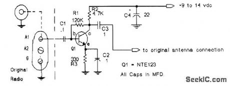
The RF broadband preamplifier uses an NPN VHF transistor as an untuned broadband (0.5 to 30 MHz) RF amplifier. Input impedance is 50Ω, allowing usage for all receiver inputs, and the unit has a 600-Ω output to match virtually all RF input circuits. The preamp delivers 30 dB of gain at 10 MHz, with a noise factor below 1 dB. Power for the preamp can be obtained from a variety of sources. The assembly requires from 9 to 14 Vdc and draws 8 mA of current. This makes it ideal for use in battery-operated portable equipment. (View)
View full Circuit Diagram | Comments | Reading(2791)
Anti-electromagnetic Interference PWM Fan Controller Circuit
Published:2011/8/4 2:39:00 Author:May | Keyword: Anti-electromagnetic Interference, PWM Fan Controller


Microchip Tech-nology ( Microchip) company provides a type of fan refrigeration speed control system series product working on PWM mode, they are used for DC brushless cooling fans ( literature cite one) . We can use outside NTC(negative temperature coefficient) thermistor or a kind of PIC microcontroller from Microchip Tech-nology and SMBus serial data bus to utilize PWM waveform's dutyfactor to control fan speed.Figure 1 shows one kind of typical application ( literature cite two) description of TC664 and TC665 controller data information. It uses 1mF frequency control capacitor CF and fan controller IC1 to generatre a PWM pulse series, its nominal frequency is 30Hz,and thedutyfactor change range rely on temperatureis 30%-100%.
(View)
View full Circuit Diagram | Comments | Reading(1968)
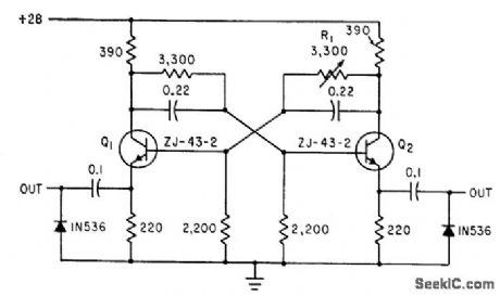
CHOKE_CONTROLLED_FREE_RUNNING_MVBR
Published:2009/7/16 5:23:00 Author:Jessie

Small resistors between chokes and ground bias transistors initially into active region to insure self-starting. Crossover resistors insure that chokes recover rapidly.-W. M. Carey, Using Inductive Control in Computer Circuits, Electronics, 32:38, p 31-33. (View)
View full Circuit Diagram | Comments | Reading(812)
| Pages:719/2234 At 20701702703704705706707708709710711712713714715716717718719720Under 20 |
Circuit Categories
power supply circuit
Amplifier Circuit
Basic Circuit
LED and Light Circuit
Sensor Circuit
Signal Processing
Electrical Equipment Circuit
Control Circuit
Remote Control Circuit
A/D-D/A Converter Circuit
Audio Circuit
Measuring and Test Circuit
Communication Circuit
Computer-Related Circuit
555 Circuit
Automotive Circuit
Repairing Circuit