
Circuit Diagram
Index 713
OUTPUT_BUFFER_AMPLIFIER
Published:2009/7/16 4:00:00 Author:Jessie
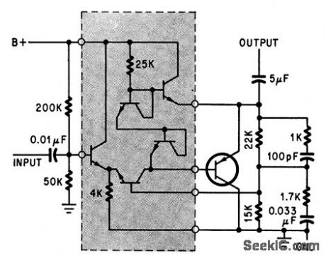
Integrated construction (shaded) is used with external pnp transistor.-D. D. Robinson, linear Microcircuits Scarce? Now You Can Breadboard Your Own, Electronics, 37:27, p 58-64. (View)
View full Circuit Diagram | Comments | Reading(764)
INVERTED_VEE_ANTENNA
Published:2009/7/13 3:36:00 Author:May

The inverted vee antenna is widely used by SWLs and radio amateurs. It has the advantage of needing only one support and can be fit into somewhat smaller spaces in some instances. A balurt having a 1:1 impedance designed for 50Ω can be installed at the feed point for improved performance, if desired.
(View)
View full Circuit Diagram | Comments | Reading(952)
ANTENNA_NOISE_BRIDGE_DETECTOR
Published:2009/7/13 3:35:00 Author:May

The circuit is illustrated in the figure. The noise output from your antenna noise bridge is applied though a coax jumper cable to J1, an SO-239. This noise, which usually will peak slightly below 1.0 V, is broadband white noise and is fed though C1, a 100-pF capacitor, to a pair of small-signal diodes connected as a rectifier/voltage doubler. The rectified dc voltage, filtered by C3, an 0.1-μF disk capacitor, is then applied to the base of a small-signal NPN transistor (Q1), which serves as a meter amplifier. Meter M1 is a 200-μA meter. It monitors collector current through Q1. On/off switch S2 is mounted on the GAIN control, which, in series with R3, forms a voltage divider across battery BT1, a 9-V battery, which powers this instrument. The GAIN control is wired so that the wiper travels from the end of R3 to ground as the krtob is rotated clockwise. This sets the emitter bias and the point at which Q1 will go into conduction as rectified noise voltage is applied to the base of Q1. The current drain from the battery is approximately 8 pA with no input, increasing to slightly over 200 μA with the meter at full scale. With such low current drain, an alkaline battery should last for years, even if you forget to turn the instrument off! This instrument covers the range from below 40 m to above 10 min two bands: 40 and 30 m, and 20-17-15-12-10 m. Bandswitch S1, an SPDT toggle or slide switch, selects the frequency range. The tuning capacitor C2 is a small 150-pF air variable. (View)
View full Circuit Diagram | Comments | Reading(1486)
THREE_RANGE_LIGHT_METER
Published:2009/7/13 3:34:00 Author:May

Uses probe containing Clairex 905HN light-dependent resistance element, connected to DC differential amplifier driving meter having specially calibrated scale. Article gives calibration procedure. Switching circuit provides constant check on voltage of 22.5-V battery. If 4.5-V battery is low,full-scale adjustment cannot be made Resistors having values specified in article are connected in turn to terminals of photocell jack P1 for calibration that gives linear scale reading.-J.L. Mills, Jr., Light Right?-Do-It-Yourself Photo Exposure Meter, 73 Magazine, Sept.1978,p 204-206 and 208-211. (View)
View full Circuit Diagram | Comments | Reading(780)
DTMF_DECODER_II
Published:2009/7/13 3:34:00 Author:May
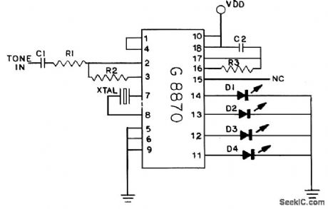
This decoder uses a 68870 DTMF receiver decoder chip to decode DTMF signals and display them in binary via LEDs. Xtal is a 3.579-MHz TV burst crystal. C1=C2=0.1μF, R1=R2=100 kΩ, and R3=300 kΩ. D1 through D4 are small red LEDs. (View)
View full Circuit Diagram | Comments | Reading(3226)
FLIP_FLOP_FOR_SHIFT_REGISTER
Published:2009/7/16 4:00:00 Author:Jessie
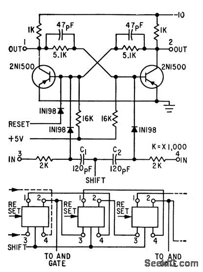
Used to pro duce complex pulse sequences up to 4 billion bits in length, at frequencies up to 1.5 Mc-Each flip-flop provides 10 ma when turned on and draws 0.6 ma when off.-B. K. Ericksen and J. D Schmidt, Random Pulse Generator Tests Circuits, Encodes Messages, Electronics, 34:25, p 56-59. (View)
View full Circuit Diagram | Comments | Reading(716)
MICROWAVE_REFLECTION_ANTENNA
Published:2009/7/13 3:33:00 Author:May
Originally used for 10-GHz microwave transmitter testing, this antenna modulates a received signal with 30 MHz and reflects it, producing a signal component 30 MHz offset from the incident signal for reception and dish-aiming tests. (View)
View full Circuit Diagram | Comments | Reading(3233)
SIMPLE_POLARITY_INDICATOR
Published:2009/7/16 4:00:00 Author:Jessie

Use this circuit to determine the polarity of low-voltage dc circuits. If the green LED lights, the red probe is positive. If the red lights, the red probe is negative. (View)
View full Circuit Diagram | Comments | Reading(1176)
BALUN_BOX
Published:2009/7/13 3:32:00 Author:May
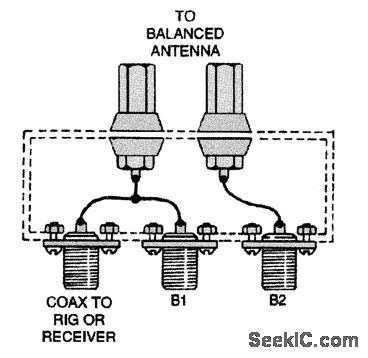
Here's the connection box for making a 4:1 coaxial balun. It is intended for mounting on antenna center isolator. (View)
View full Circuit Diagram | Comments | Reading(813)
10_GHz_WAVEGUIDE_TEST_ANTENNA_SETUP
Published:2009/7/13 3:31:00 Author:May
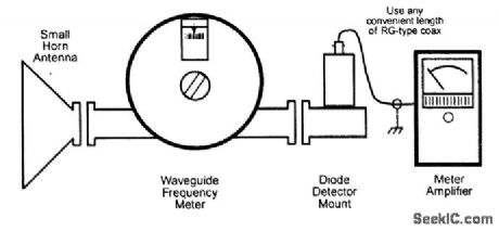
This waveguide test antenna, wavemeter, and meter amplifier setup uses a small horn antenna and a variable commercial waveguide frequency meter to determine RF frequency. RF is sampled with a detector and displayed on an amplified meter for sensitive meter indications. (View)
View full Circuit Diagram | Comments | Reading(855)
165_MHz_TO_135_kHz
Published:2009/7/16 4:00:00 Author:Jessie

Provides good selectivity, good AVC, and smooth tuning.Article gives coil-Winding data,-B. Hoisington, Miniboxing the 432er Receiver, 73 Magazine, Jan,1975、p46-52, (View)
View full Circuit Diagram | Comments | Reading(1148)
OP_AMP_ANTENNA_AMPLIFIER
Published:2009/7/13 3:30:00 Author:May
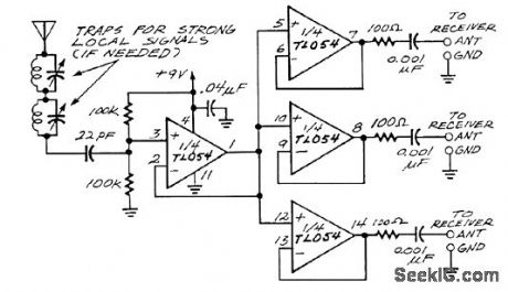
The impedance of a random-wire antenna at broadcast-band frequencies will be several kilohms, a poor match for the 50-Ω input of a receiver. Also, the inputs of multiple receivers can't be connected directly to a single antenna, or they'll detune each other. The circuit solves both problems. The first op amp overcomes the impedance mismatch, strengthening the signal greatly even though it has no voltage gain. The rest of the op amps feed the signals to the separate receivers. No low-pass filter is needed because the gain of these op amps drops off sharply above 2 or 3 MHz. (View)
View full Circuit Diagram | Comments | Reading(1370)
SIMPLE_LAMP_DRIVER
Published:2009/7/13 3:30:00 Author:May

Small current through the base controls large current through the collector.Close the switch,and the bulb lights. (View)
View full Circuit Diagram | Comments | Reading(718)
HIGH_GAIN_AUDIOPREAMP
Published:2009/7/16 3:59:00 Author:Jessie
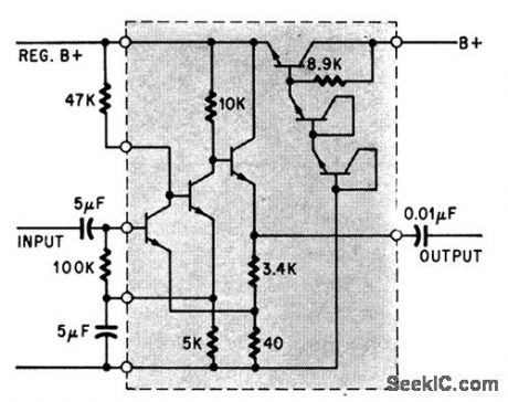
Has strong negative feedback and built-in power supply series regulator.-D. D. Robinson, Linear Microcircuits Scarce? Now You Can Breadboard Your Own, Electronics, 37:27, p 58-64. (View)
View full Circuit Diagram | Comments | Reading(580)
LOW_POWER_ANTENNA_TUNER_AND_SWR_METER
Published:2009/7/13 3:28:00 Author:May

The SWR meter is a variation of a resistive bridge. This circuit has the advantage of providing high sensitivity at low power inputs. Its disadvantage is that the maximum power that can be applied to the circuit is limited by the power dissipation of the 50-Ω bridge resistors because 75 percent of the transmit power is absorbed by these resistors under perfectly matched conditions. In this circuit, a DPDT switch adds in a 100-Ω resistor only for SWR readings, allowing the circuit to provide a reasonable SWR for your transmitter even during severe tune-up conditions. Additionally, you have minimum insertion loss in the FORWARD position because the l-kΩ bridge resistors permit you to always indicate forward relative power and calibrate the full-scale reading for SWR measurements. The antenna tuner itself is a standard T-type tuner utilizing a pair of 335-pF miniature transistor radio variable capacitors and a toroidal inductor, tapped as shown in the figure. To actually make the taps, simply wind the toroid with 40 turns of #24 wire, and then scrape the outer surface of each appropriate tum with a hobby knife to clean off the enamel insulation. Then tin each wire turn, and tack-solder tap wires to them. (View)
View full Circuit Diagram | Comments | Reading(3332)
METAL_FORMING_CONTROL
Published:2009/7/13 3:27:00 Author:May


Determines yield point by sensing when tension and elongtion begin increasing at different rate during stretching and forming. Elongation signal comes from potentiometer R1, linked to ram of hydraulic relief valve. Tension signal comes from strain-gage bridge that delivers 0 to 10MV at 60 cps. At yield point.system lowers tension as dies are applied to metal. At end of cycle, operotor opens stop switch, resetting relays that are energized by power line.-G. J. Crowdes, Aulomalic Controls for Metal Working Machines.Electronics.32:10,p41-43. (View)
View full Circuit Diagram | Comments | Reading(805)
COMPLEMENTARY_TRANSISTOR_LOGIC
Published:2009/7/16 3:59:00 Author:Jessie

Uses both pnp and npn transistors, with pnp emitters tied together and returned through 1K resistor to positive voltage supply. Propagation delay is 3 to 5 nsec for fanouts of 1 to 10.-D. Christiansen, Logic Schemes Reviewed, EEE, 13:11, p 64-79, (View)
View full Circuit Diagram | Comments | Reading(662)
ANTENNA_TUNING_INDICATOR
Published:2009/7/13 3:27:00 Author:May

The stealth antenna tuning indicator consists of a sensitive reflected-power bridge and indicator (R2 to R6 and associated components) and a switch (S1) that lets you route your transceiver's power into a dummy antenna (TUNE) or your antenna system (OPERATE). One more component, R1 (a resistance cortsisting of two separate 3-W resistors, R1A and R1B), leaks just enough of your transmitter's power to the bridge and your antenna system to allow low-interference tune-up when S1 is set to TUNE. (View)
View full Circuit Diagram | Comments | Reading(1730)
LED_SWR_INDICATOR_CIRCUIT
Published:2009/7/16 3:59:00 Author:Jessie


D1 and D2 act as half-wave diode detectors for the forward and reverse voltages. In traditional SWR-meter circuits, the output of these detectors feeds a panel meter via a forward/reflected switch and a scaling resistor, which typically provides the detector diodes with a load on the order of 25 kΩ. This relatively low load impedance limits the diodes' performance at low power levels because it causes their forward voltage drop to be higher than the sampled RF voltages to be detected. To use LEDs (DS1 and DS2) as indicators, some sort of dc amplifier was needed. Operational amplifiers were used because their high input impedance lets us load the diodes so lightly that their detection range can extend down to about 50 mV. U1A and U1B, halves of a TL072 dual JFET-input op amp, do the dc amplification. The dc voltage developed by each detector is presented to its op amp across a 5.6-MΩ resistor. Each op amp operates at a voltage gain of 1 (unity), but provides enough current gain to drive an LED and to cause a matching voltage to appear across R3. To provide each half of U1 with split (positive and negative) power supplies in environments in which only single-polarity, negative-ground supplies are typical, it was necessary to provide an artificial ground. U2 provides a stiffly regulated dc voltage between ground and the positive supply. (Note that the bridge circuit's dc reference is also set to +5V because the RE-grounded end of L1, which is connected to dc ground in traditional directional-watt meter circuits, is also connected to the +5-V supply provided by U2.) The overall sensitivity of the circuit can be adjusted to match the power level expected by changing the values of R3 and R4 to drive the LEDs with an appropriate current level. If you use different LEDs or want to use the bridge at a different power level, you may want to adjust these resistor values ac-cording to the formula R3 and R4 (ohms)=√P0×50/30×If(LED) ,where P0 is the transmitter power in watts, 50 is the system impedance in ohms, 30 is T1's turns ratio, and If(LED) is the current level (in amperes) that produces the LED brightness you need. With the resistor values chosen to light the FED LED (DS2) brightly, the REV LED (DS1) will be easily visible at SWRs around 2:1, allowing no-guess SWR dipping with tuner adjustment. (View)
View full Circuit Diagram | Comments | Reading(2786)
DTMF_DECODER_I
Published:2009/7/13 3:27:00 Author:May

This decoder uses a G8870 DTMF receiver decoder chip to decode DTMF signals and display them via an LED display driven by a 7448 decoder driver chip. Xtal is a 3.579-MHz TV burst crystal.C1=C2-0.1μF, R1=R2=100 kΩ.and R3=300 kΩ. D1 through D4 are small red LEDs. (View)
View full Circuit Diagram | Comments | Reading(6665)
| Pages:713/2234 At 20701702703704705706707708709710711712713714715716717718719720Under 20 |
Circuit Categories
power supply circuit
Amplifier Circuit
Basic Circuit
LED and Light Circuit
Sensor Circuit
Signal Processing
Electrical Equipment Circuit
Control Circuit
Remote Control Circuit
A/D-D/A Converter Circuit
Audio Circuit
Measuring and Test Circuit
Communication Circuit
Computer-Related Circuit
555 Circuit
Automotive Circuit
Repairing Circuit