Circuit Diagram
Index 705
SENSITIVE_RELAY_CONTROL
Published:2009/7/13 4:20:00 Author:May

Reflex circuit ensures full use of available gain of two-stage relay control ampliler using 12AT7 twin-triode. Tube V2 controls relay in its plate circuit and also serves as a-c amplifier, increasing over-all sensitivity by factor approximately equal to a-c gain. Performs best about 400 cps.-Sensitive Relay Control Amplifier, Electronic Circuit Design Handbook, Mactier Pub. Corp.,N.Y.,p103. (View)
View full Circuit Diagram | Comments | Reading(619)
SOUND_LEVEL_METER
Published:2009/7/16 4:44:00 Author:Jessie

Power for the circuit is provided by B1, a 9-V battery. Total battery current is 14.5 mA, so an alkaline battery should last about 250 hours. Audio signals are picked up by microphone MIC1. The output of MIC1 is buffered by Q1 to maintain the 3000-Ω load of resistor R2. The input impedance at pin 16 of the NE614 (U1) is 1600Ω to reduce the gain on the high end and preserve the RSSI linearity. The RSSI signal is a current source that flows through R6 to establish a voltage at pin 5 of U1;the RSSI output voltage is a function of the input SPL. Capacitor C10 removes high-frequency components. The slope of the RSSI line is nominally 0.084VCC/10 dB. Op amp U2-b is configured as a non-inverting voltage buffer with a gain of 1.2; multiplied by the RSSI slope, this produces a slope of 0.1VCC/10 dB. The display, DISP1, is a 10-bar LED that is used to indicate sound level in 10-dB increments from 30 to 120 dB(A). The display is driven by an LM3914linear bar-graph driver, U5. The internal voltage regulator of U5 functions by establishing a constant current through R15 because the voltage between pins 7 and 8 is maintained at 1.25V. The resulting voltage at the emitter of Q2 is about 5V, which powers U1, U3, and the internal voltage-divider string of U5 at pin 6. Each segment of the display will increase by 10 dB, independent of the exact magnitude of VCC While the slopes of the display driver and the RSSI signal are the same, they might not have the sanit offset. For that reason, an LM334, U4, is used to source a constant 10-μA current through R17 to generate a fixed off-set voltage on top of the composite RSSI voltage at the output of U2-a. By adjusting the value of potentiometer R17, differences in microphone sensitivity can be accommodated so that the display reads properly from 30 to 120 dB(A). The proper readout of the display is also ensured by an ICM7555 timer, U3, which is configured as a self-excited square-wave oscillator; the resulting peak-Lo-peak, 1-kHz signal of the timer is almost one step size of DISP1. (View)
View full Circuit Diagram | Comments | Reading(0)
4_W_WIDE_BAND_AMPLIFIER
Published:2009/7/13 4:20:00 Author:May

Uses complementary transistors for operation up to 100 kc with low distortion. Output is class B.All leads should be kept shott, to minimize tendency to oscillate.-N. Freyling, A 4-Watt Wide-Bond Solid-State Amplifier, Motorola Application Note AN-209, Mar.1966. (View)
View full Circuit Diagram | Comments | Reading(737)
CODE_COMPARATOR
Published:2009/7/16 4:45:00 Author:Jessie

Identifies preselected code pulse train while rejecting incorrect or extraneous signals, to give distinctive marker on radar ppi when desired one of ten coded video replies is received. Thumbwheel code selection switches on beacon control box determine which code is to be recognized.-W. L. Woodson, Automatic Beacon Radar Identifies Aircraft, Electronics, 34:6, p 57-61. (View)
View full Circuit Diagram | Comments | Reading(580)
MULTIFLASH_SWITCH
Published:2009/7/13 4:20:00 Author:May

When ramp output of flash trigger circuit (given in article) is applied to input at A, flash at output of switch circuit is tripped when ramp voltage reaches level determined by setting of R12. Similar voltage-operated switches are required for other flashes.Used for taking sequence photographs such as springboard diver in flight. Settings of R12 for diferent switches are chosen for equal times between flashes, with intervals from 11 ms to 11 s. Article gives all circuits and set up procedure.Regulated 19.5-V supply is required-R. Lewis, Multi-Flash Trigger Unit, Wireless World, Nov.1973, p 529-532. (View)
View full Circuit Diagram | Comments | Reading(866)
FM_TOUCH_TUNE
Published:2009/7/13 4:19:00 Author:May

Up to 10 channels can be tuned by turning on appropriate section of 4016 CMOS digital IC by finger contact that drives clock inhibit line low. 4017B then counts clock pulses until desired output goes high. C1 and R5 ensure that channel 0 is selected when circuit is turned on. Clock frequency is not critical and can range from 100 Hz to 19 kHz. For 120-Hz clock, wind several extra turns around power transformer of receiver and feed this voltage to bridge rectifier.-L. Crampin and R. van der Molen, Touch-Tune for F.M. Receivers, Wireless World, Jan. 1978, p 60. (View)
View full Circuit Diagram | Comments | Reading(705)
VOLTAGE_CONTROLLED_PULSE_SPACING
Published:2009/7/16 4:41:00 Author:Jessie


Unijunction transistor circuit generates train of pulses with constant pulse width but with spacing linearly adjustable over 20.to-1 rang by voltage V, which varies trigger point of uit Q2.-A. M. Ridenour and F. Turco, Unijunction Controls Spacing Between Pulses, Electronics, 39:14, p 82-83. (View)
View full Circuit Diagram | Comments | Reading(803)
10_POINT_STEPPER
Published:2009/7/13 4:19:00 Author:May

4017 divide-by-10 counter routes input clock signal sequentially to each of ten output lines, with only selected output going high. Intemal circuit of IC is self-clearing walking ring that is glitch-free, with minimum overlap between outputs. Counters can be cascaded to provide more steps. -D. Lancaster, CM0S Cookbook. Howard W. Sams, Indianapolis, IN, 1977, p 309. (View)
View full Circuit Diagram | Comments | Reading(726)
PULSE_CODED_100_WATT_BEACON
Published:2009/7/16 4:41:00 Author:Jessie

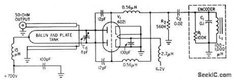
Push-pull power oscillator with transmission-line tank gives good frequency stability at 220 to 260 Mc. Encoder uses capacitor charge and discharge to cut off V1 at intervals giving pairs of 10-microsec pulses to aid in recovery of spacecraft.-J. G. Richter, Redesigning Project Mercury Beacons, Electronics, 35:3, p 50-52. (View)
View full Circuit Diagram | Comments | Reading(690)
LAMTERN_BATTERY_EXTENDER_
Published:2009/7/13 4:19:00 Author:May

Life of lanternbattery can be tripled without reducing light by chopping current while doubling voltage at 50% duty factor. 6-V lamp is connected across chopped 12-V supply built around 4011 CMOS quad NAND gate. First two gates form chopping oscillator, while third serves as interface to any NPN high-gain power transistor. If lamp draws more than 1 A, add fourth gate as shown in dashed lines. If gate is not used, tie its input Ieads to pin 14 of IC. Duty cycle is varied with 1-megohm pot; set at midrange before ap-plying power, then adjust for normal lamp bril-liance.-J. A. Sandler, 9 Easy to Build Projects under $9, Modem Electronics, July 1978, p 53-56.
(View)
View full Circuit Diagram | Comments | Reading(697)
PULSE_SQUARING_ZENERS
Published:2009/7/16 4:38:00 Author:Jessie

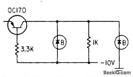
Addition of zener diodes lo transistor amplifier fed by tunnel.diode pulse generator improves output wave form.-G. B. Smith, Tunnel Diode Generates Rectangular Pulses, Electronics, 33:48, p 124-l25. (View)
View full Circuit Diagram | Comments | Reading(718)
ADJUSTABLE_INPUT_IMPEDANCE
Published:2009/7/13 4:18:00 Author:May

Q4, Q1, and Q2 in negative feedback loop encompass Q2 and Q3 in positive loop, to give stoble amplifier with input conductance of zero (infinite impedance) and unity gain for almost any output load, with output of l0 v p-p at 1 ma.-R. L. Willett, Positive and Negative Feedback Multiply Amplifier Input Impedance, Electronics, 34:27, p 52-53. (View)
View full Circuit Diagram | Comments | Reading(676)
ANTICOINCIDENCE
Published:2009/7/13 4:18:00 Author:May

Developed for use with bidirectional counter circuits to avoid counting errors when up and down pulses occur simultaneously. Operation is based on knowing maximum frequency of separate data pulses. Outputs 1 and 2 will be separated by at least one clock period even if inputs D1 and D2 occur simultaneously. Article gives operating details. -J. H. Burkhardt, Jr., Anti-Coincidence Circuit Prevents Loss of Data, EDN|EEE Magazine, Jan. 1, 1972, p 73. (View)
View full Circuit Diagram | Comments | Reading(1753)
AM_RADIO
Published:2009/7/16 4:32:00 Author:Jessie

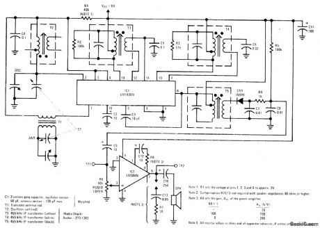
National LM1820N IC provides all sections of superheterodyne broadcast-band radio up to second detector, with diode and power opamp forming rest of receiver. Output is 1/4 W into 8-ohm loudspeaker when operating from 6-V supply. Total current drain is about 10mA, making battery operation feasible.-E. S. Papanicolaou and H. H. Mortensen. Low-Cost AM-Radio System Using LM1820 and LM386, National Semiconductor, Santa Clara, CA, 1975, LB-29. (View)
View full Circuit Diagram | Comments | Reading(0)
TOUCH_CONTROLLED_RELAY
Published:2009/7/13 4:17:00 Author:May

Basic circuit uses Signetics 555 timer to make LED flash each time input is touched with finger. Replace LED with flip-flop (any type) and three sections of 8T90 hex power inverter to drive DC relay. Silicon diode suppresses voltage spikes generated when magnetic field of relay collapses. Use only as many paralleled sections of inverter as are required to operate relay. Input can be brass or copper plate at least 2 inches square.-G.Young, Voltage, Current, and Power Supplies, Kilobaud, Nov. 1977, p 76-78 and 80-82. (View)
View full Circuit Diagram | Comments | Reading(907)
BASIC_555_TIMER
Published:2009/7/13 4:17:00 Author:May

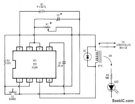
Closing switch S1 momentarily applies activating signal to trigger input pin 2 of timer, to start charging of C1. When C1 charges to two-thirds of supply voltage, timer discharges it to complete timing cycle. Duration of charging interval can be varied from several microseconds to over 5 min by changing values of R1 and C1. With 1K for R1, capacitor values of 0.01 to 100 μF give time range of 10μs to 100 ms. With 100 megohmsand lμF,time increases to 10s. Once timer starts, closing S1 again has no effect. Timing cycle can be interrupted only by applying reset pulse to pin 4 or opening power supply. Circuit will drive LED directly or can be used with miniature relay (Radio Shack 275-004) to control larger loads. Can be used as darkroom timer if LED is kept several feet away from photographic paper. Diode is 1N914.-F.M, Mims, Integrated Circuit Projects, Vol. 2, Radio Shack, Fort Worth, TX, 1977, 2nd Ed., p 57-65. (View)
View full Circuit Diagram | Comments | Reading(1314)
VOICE_STRESS_ANALYZER
Published:2009/7/16 4:31:00 Author:Jessie

This circuit analyzes the 7-to 15-Hz voice-frequency components that are associated with the stressed voice that occurs if a person is lying or under duress of some kind. These components appear as an amplitude modulation on the voice and are thought to be inversely proportional to psychological stress. Their relative amplitudes are read out on a bar-graph display. (View)
View full Circuit Diagram | Comments | Reading(1605)
PASSIVE_REDUNDANCY_IN_A_C_AMPLIFIER
Published:2009/7/13 4:17:00 Author:May

Uses two amplilers connected in parallel on individuol-stage basis, with 1K isolation resistors between stages. Amplifier is operational type having closed-loop gain of 10, open-loop gain of 1,000, and 3-db open-loop frequency response from 30 to 1,500 cps.Both open-loop gain and frequeney response are functions of failure mode of circuit, with most types of failure affecting performance only slightly.-T. B. Booker, Designing Redundant Analog Amplifiers, EEE, 13:2, p 55-59. (View)
View full Circuit Diagram | Comments | Reading(821)
PROM_CONTROLLED_COUNTER
Published:2009/7/13 4:16:00 Author:May


Universal counter can be set to count in any desired se-quence ranging from simple binary to pseudorandom, using only one programmable read-only memory chip and one 74174 edge-triggered flip-flop register chip, Version shown is 6-bit 64-state counter for which PROM is organized in 64 8-bit words. Pull-up resistors are required. Article covers application details, in-cluding expansion techniques. PR0M outputs serve as data input to register chip, and register outputs provide PR0M address inputs. -T. M. Farr, Jr., Read-only Memory Controls Universal Counter, EDN Magazine, May 5, 1976, p 114. (View)
View full Circuit Diagram | Comments | Reading(985)
3_LIGHT_SUPERHET_MARKER_BEACON
Published:2009/7/16 4:30:00 Author:Jessie

Gives audio output as well as colored-light presentation in aircraft. Superheterodyne provides immunity to spurious activation of lamps by tv stations.-F. P. Smith, Transistorized Receiver for Marker Beacon Use, Electronics, 37:46, p 76-78. (View)
View full Circuit Diagram | Comments | Reading(1297)
| Pages:705/2234 At 20701702703704705706707708709710711712713714715716717718719720Under 20 |
Circuit Categories
power supply circuit
Amplifier Circuit
Basic Circuit
LED and Light Circuit
Sensor Circuit
Signal Processing
Electrical Equipment Circuit
Control Circuit
Remote Control Circuit
A/D-D/A Converter Circuit
Audio Circuit
Measuring and Test Circuit
Communication Circuit
Computer-Related Circuit
555 Circuit
Automotive Circuit
Repairing Circuit