
Circuit Diagram
Index 717
STEPPING_SWITCH_PULSER
Published:2009/7/16 5:48:00 Author:Jessie

Used to advance stepping switch automatically at predetermined rate, in automatic test equipment providing go-no-go indications. C1 controls output pulse wideth to give 80-msec on time, for reliable actuation of switch that normally requires 20 millisec. Rang of off time, controlled by R5 , is 20 millisec to 7 sec.-.Wilson Step Switch Pulser, EEE, 10:11, P 26-27 . (View)
View full Circuit Diagram | Comments | Reading(734)
CASCADED_MMIC_AMPLIFIER_CIRCUIT
Published:2009/7/13 3:01:00 Author:May
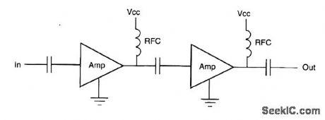
Most MMIC amplifliers can be cascaded, with dc blocking as the only interstage connection requirement. (View)
View full Circuit Diagram | Comments | Reading(1515)
10_MHz_FIXED_FOR_WWV
Published:2009/7/16 5:47:00 Author:Jessie

Fixed-frequency receiver has high sensitivity, portability, low power consumption, and low cost. Number of time parts is minimized by using RCA CA3088 IC for converter, lF, detector, audio preamp, AGC, and tuning-meter output, along with RCA CA3020 as audio amplifier. Table gives crystal frequencies and tuned-circuit values for all nine frequencies on which frequency calibration data, propagation forecasts, geophysical alerts, time signals, and storm warnings are broadcast by American and Canadian governments. Core type numbers are for Amidon Associates cores. IF transformers come as Radio Shack set 273-1383; use only T1 (gray core) and T2 (white core). Specify load capacitance as 32 pF when ordering crystals. Use overtone crystals for 20 and 25 MHz with C5 replaced by short and C6 reduced to 10 pF.-A. M. Hudor, Jr., Fixed. Frequency Receiver for WWV, Ham Radio, Feb.1977, p 28-33. (View)
View full Circuit Diagram | Comments | Reading(2412)
COMBINED_MMIC_AMPLIFIERS
Published:2009/7/13 3:00:00 Author:May
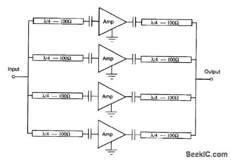
Quadrature combining, practical in microstrip, can be used to obtain a medium power output from several MMIC amplifiers. (View)
View full Circuit Diagram | Comments | Reading(780)
TRANSDUCER_VOLTAGE_RESISTANCE_CONVERTER
Published:2009/7/16 5:47:00 Author:Jessie

D-c voltage output of transducer is converted to a-c voltage by fet in one leg of bridge that controls f-m oscillator.Arrangement converts transducer in effect to variable resistor, simplifying measurement of many parameters in data acquisition system.-A. R. Greenfield and W. H. McCloskey, FET Converts Transducer for Use in A-C Bridge Electronics, 39:3, p 84-85. (View)
View full Circuit Diagram | Comments | Reading(1200)
LOW_NOISE_DC_TO_DC_CONVERTER
Published:2009/7/13 3:00:00 Author:May

Low noise is achieved by this inexpensive and versatile 5-V-to-±12-V dc-to-dc converter. Wide-band output noise appears to be well under 500 μV p-p. The converter accepts external clocks from 80 to 120 kHz. The converter operates much like a TV horizontal deflection circuit. Q3 is a logic-level power MOSFET driven by an external clock. When Q3 is switched on, current ramps up through T1's primary. When Q3 is switched off, Q3's drain flies back to 25 Y as C4 resonates with T1's primary, transferring energy to the secondary. As the flyback voltage falls and attempts to go below ground, the intrinsic diode of the power MOSFET clamps it. In addition, the excess resonant energyflows backward through T1's primary, recharging C1. When this point is reached, Q3 is again switched on and the cycle repeats. Q3's gate (trace 2) is switched on and off when Q3's drain is near ground. Q3's gate driver power requirements are modest enough to be handled by any 74HC logic gate. Regulation is achieved by the error amplifier (LT1013). Despite the fact that Q1 acts as a linear pass transistor, converter efficiency can exceed 75 percent if the voltage drop across Q1 is minimized. This can be accornplished by either adjusting the clock frequency or tuning C4 to adjust the flyback voltage. (View)
View full Circuit Diagram | Comments | Reading(2966)
5_V_TO_4_V_CONVERTER
Published:2009/7/13 2:57:00 Author:May

Generating a 4-V supply voltage for some of the new microprocessors from a 5-V main requires a low-voltage-loss capability in an efficient switching power supply. The LTC1147L circuit shown provides this capability in only 0.6 in2 of board space. The LTC1147L is a high-efficiency step-down switching regulator controller that provides gate drive control for an external P-channel MOSFET switch. Up to 100 percent duty cycle is possible with the LTC1147L, allowing the output voltage to be close to the input voltage. This device uses a constant off-time architecture and can operate at switching frequencies eiceeding 400 kHz. The LTC1147L is an adjustable device, with the output voltage set by an external resiator divider network. Maximum load current is set by the value of the current sense resistor R2. (View)
View full Circuit Diagram | Comments | Reading(791)
ULTRA_LONG_MONO
Published:2009/7/16 5:46:00 Author:Jessie

Has quiescent power drain of zero. Generates step-function gate with good leading and trailing edges, and provides delayed pulse of either polarity for triggering cascaded circuits. Q1 is 2N1442, scr Q2 is 2N1595 or 3A31, and ujt Q3 is 2N489. Values for R3 and C2 give 50-sec pulse duration.-Ultra-Long Monostable Multivibrator, Electronic Circuit Design Handbook, Mactier Pub. Corp., N.Y., 1965, p 66. (View)
View full Circuit Diagram | Comments | Reading(931)
TRIAC_LAMP_DIMMER
Published:2009/7/13 2:57:00 Author:May
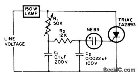
Can easily be buih into lamp socket or fixture. Uses minimum number of components.-J. Eimbinder, SCRs In the Consumer Market, EEE, 14:8, p100-103. (View)
View full Circuit Diagram | Comments | Reading(1363)
SCR_LAMP_DIMMER
Published:2009/7/13 2:55:00 Author:May
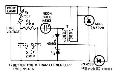
Can easily be built into lamp socket or fixtore.-J. Eimbinder, SCRs in The Consumer Market, EEE, 14:8, p100-103. (View)
View full Circuit Diagram | Comments | Reading(898)
PULSE_CLAMP
Published:2009/7/16 5:46:00 Author:Jessie

Clamps pulses in millivolt range to any d-c level even though pulses are below barrier potentials. Also used for sampling pulse amplitudes and for storing sampled amplitude in memory capacitor.-A. J. Koll, E. Bleckner, and O. C. Srygley, Semiconductor Clamp Handles Millivolt Signals, Electronics, 33:35, p 64-65. (View)
View full Circuit Diagram | Comments | Reading(798)
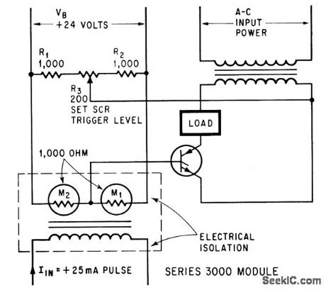
INPUT_PULSE_UNBALANCES_BRIDGE
Published:2009/7/16 5:45:00 Author:Jessie

Trigger pulse causes opposite resistance variations in magnetoresistors M1 and M2, to give 1 v output for 25-ma pulse current.-R. M. Gitlin, Magnetoresistors Isolate Load From Control Circuit, Electronics, 38:3, p 60-61. (View)
View full Circuit Diagram | Comments | Reading(988)
D_C_LEVEL_SHIFTER
Published:2009/7/16 5:43:00 Author:Jessie

Bridge R1D5R2D6 and two transistors in d-c negative-feedback loop deliver output signal that is replica of input but at lower impedance and shifted in d-c voltage level a predetermined amount.-J. Willis, High Precision D-C Level Shifter Reduces Output Impedance, Electronics, 36:18, p 65-68. (View)
View full Circuit Diagram | Comments | Reading(1291)
TRANSISTOR_BRIDGE_SWITCHES_MICROVOLT_SIGNALS
Published:2009/7/16 5:42:00 Author:Jessie

Circuit approaches infinite impedance during off condition by lowering emitter-to-collector conductance gap to zero. Conventional reset flip-flop controls on and off operation of series-connected npn and pnp bridge transistors. –M.V. Kalfaian, Transistor Bridge Switches Microvolts, Electronics, 37:1, p 60. (View)
View full Circuit Diagram | Comments | Reading(832)
CHART_RECORDER_RANGE_EXTENDER
Published:2009/7/16 5:41:00 Author:Jessie

The circuit diagram shown was designed to adapt a laboratory chart recorder with a 100-mV in-put for full-scale deflection so that it will accept input voltages of 1V, 2V, 5V, or 10V at the flick of a switch. The op amp (IC1) is configured as an inverting amplifier whose feedback resistance is much less than the input resistance (R1); therefore, the output voltage will be a fraction of the input signal. Range switch S1 selects among four different feedback resistors, which consist of fixed metal-film resistors and a 20-turn cermet trimmer, which is adjusted to produce 100 mV output at the selected input voltage range. In practice, VR2 should be adjusted to 100 mV output at 2V input. The other ranges are set up in the same manner. (View)
View full Circuit Diagram | Comments | Reading(1383)
CRYSTAL_PARAMETER_BRIDGE
Published:2009/7/16 5:41:00 Author:Jessie

Bridge plugs into crystal socket of standard crystal impedance meter, and crystal under test plugs into bridge. Only other instruments needed for measuring equivalent parameters of overtone crystals for 75 to 200 Mc are frequency meter and null-indicating meter.-D. W. Robertson, Plug-in Bridge Checks VHF Quartz Crystals, Electronics, 31:19, p 82-85. (View)
View full Circuit Diagram | Comments | Reading(1259)
SCR_CONTROL
Published:2009/7/16 5:40:00 Author:Jessie
Firing angle and trigger level are controlled by magnetoresistor bridge.-R. M. Gitlin, Magnetoresistors Isolate Load From Control Circuit, Electronics, 38:3, p 54-59. (View)
View full Circuit Diagram | Comments | Reading(780)
FOUR_CELL_TO_5_VDC_CONVERTER
Published:2009/7/13 2:54:00 Author:May

Generating a regulated 5-V output frorrt a four-cell NiCd battery pack requires step-down opera-tion when the battery voltage is above 5 V (fully charged pack at 6 V) and step-up operation when the battery voltage drops from 5 V to 3.6 V during discharge. The LT1373 converter circuit shown achieves up to 83 percent efficiency at high current (100- to 200-mA range), better than a flyback approach. The 250-kHz switching frequency minimizes inductor values, and both 33-μH inductors are wound on the same core, requiring less board area. With a quiescent current of I mA typically, the LT1373 offers high efficiency at high frequency, extending the battery lifetime in applications. (View)
View full Circuit Diagram | Comments | Reading(943)
SELF_BALANCING_TORQUE_INDICATOR
Published:2009/7/16 5:40:00 Author:Jessie

Uses shunt bridge balancing technique. Amplifier and servo motor that drive 50-ohm balancing pot RB are standard commercial units. Highly stable power supply and reference voltage are not needed.-C. H. Haakana, Shunt Bridge Balancing in Strain-Gage Indicators, Electronics, 32:30, p 50-51. (View)
View full Circuit Diagram | Comments | Reading(927)
SIMPLE_5_V_TO_33_V_CONVERTER
Published:2009/7/13 2:53:00 Author:May
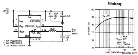
In portable logic systems requiring mixed 5-V and 3.3-V supplies, space and efficiency are paramount. Enter the LTC1574-3.3, a small and simple solution that provides over 90 percent efficiency.The LTC1574-3.3 features an intemal Schottky diode, reducing the external component count to just three parts. This high-efficiency circuit uses all surface-mount components, and employs Burst Mode operation to extend high efficiency to low current levels (see graph). A low-loss internal power MOSFET (RDS = 1.2 Ω is typical for this circuit) switch and constant off-time architecture are key in achieving this high efficiency. The LTC1574 can be shut down, limiting the supply current to 25 μA (max). (View)
View full Circuit Diagram | Comments | Reading(677)
| Pages:717/2234 At 20701702703704705706707708709710711712713714715716717718719720Under 20 |
Circuit Categories
power supply circuit
Amplifier Circuit
Basic Circuit
LED and Light Circuit
Sensor Circuit
Signal Processing
Electrical Equipment Circuit
Control Circuit
Remote Control Circuit
A/D-D/A Converter Circuit
Audio Circuit
Measuring and Test Circuit
Communication Circuit
Computer-Related Circuit
555 Circuit
Automotive Circuit
Repairing Circuit