
Circuit Diagram
Index 703
CB_CONVERTER
Published:2009/7/13 4:38:00 Author:May

Uses tunnel-diode oscillator.- Transistor Manual, Seventh Edition, General Electric Co,1964, p358. (View)
View full Circuit Diagram | Comments | Reading(912)
CLEAN_RESET
Published:2009/7/13 4:37:00 Author:May

Adding latch consisting of two 7400 NAND gates to reset circuit of divide-by-77 counter guarantees good reset. Reset pulse will always be half a clock period wide. -E. E. Hriv-nak, House Cleaning the Logical Way, 73 Mag-azine, Aug. 1974, p 85-90. (View)
View full Circuit Diagram | Comments | Reading(776)
MOSFET_GATE_DRIVER
Published:2009/7/13 4:37:00 Author:May

This ratiometric 20-kHz voltage-to-frequency converter(VFC) provides superior performance with strain gauges and other ratio-responding transducers,even with noisy, unregulated excitation voltages. Feedback isn’t used to achieve the excellent 4-Hz linearity,so there is very low frequency jitter-period measurements can be used to get several digits of resolution even when operating at a fraction of full scale. An operational synchronizing transistor starts the VFC with zero charge at the beginning of each count Cycle,eliminating the characteristic digit jumping often encountered with VFC designs. Good linearity is attained by making the comparator’s reference voltage vary with the input voltage, which precisely compensates for the finite capacitor reset Lime∶ Period=t1+t2 =t1+(Vcc-Vref)/AVin =[t1AVin+Vcc-Vref)/AVinwhere AVin=ΔV/Δt. If Vref is made to include the amount t1AVin, then the effect of t1 is eliminated∶ Period=[t1AVin+VCC-(t1AVin+Vref)]/AVinThe MPSA-18 is a remarkably high-gain transistor,even at low currents,giving good currentSource linearity down to 0 Hz. In addition,bipolar transistors work well with the low collector voltages encountered In this single-supply,10-V design . Moreover,most single-supply op amps will work in place of the LM10. But the LM10 also has a reference amplifier that could be used to construct a 10-V excitation regulator . The LM311 propagation delay gives a reset pulse width near 400 ns,which gives the transistor time to discharge the capacitor. Also,the 311’s bias current gives a small negative offset that ensures a 0-Hz output for0 V in.
(View)
View full Circuit Diagram | Comments | Reading(1609)
OTL Negative Gate Voltage Doubler Rectifier Circuit (For Tube Amp)
Published:2011/7/17 21:29:00 Author:Felicity | Keyword: OTL Negative Gate Voltage, Doubler Rectifier Circuit, (For Tube Amp)

View full Circuit Diagram | Comments | Reading(2156)
CONSTANT_BRIGHTNESS_LED_CIRCUIT
Published:2009/7/13 4:36:00 Author:May

This setup ensures that the LED will glow with equal brightness as long as the input voltage remains between 8 and 24 V. R=5/I, where I=desired LED current. (View)
View full Circuit Diagram | Comments | Reading(854)
BAR_GRAPH_DISPLAY_CIRCUIT
Published:2009/7/13 4:36:00 Author:May

This shows how an LM3914 or LM3915 is connected for 9- to separate LEDs or part of an integral display module. (View)
View full Circuit Diagram | Comments | Reading(1574)
Commonly Used High-voltage Doubler Circuit (For Tube Amp)
Published:2011/7/17 21:16:00 Author:Felicity | Keyword: Commonly Used, High-voltage Doubler, Circuit, (For Tube Amp)

View full Circuit Diagram | Comments | Reading(2962)
LARGE_LED_DISPLAY
Published:2009/7/13 4:35:00 Author:May

National MM5736 calculator chip is used with DM8895 segment driver that can be mask-programmed to source several values of current in range from 5 to 17 mA per segment of LED display, permitting use of fairly large display. Display current comes from VCC supply terminal of DM8895 rather than from calculator chip. Combination serves as 6-decade counter driving 6-digit display. -M. Watts, Calculator Chip Makes a Counter, Na-tional Semiconductor, Santa Clara, CA, 1974, AN-112, p 3. (View)
View full Circuit Diagram | Comments | Reading(1479)
50_MC_POWER_AMPLIFIER
Published:2009/7/13 4:35:00 Author:May
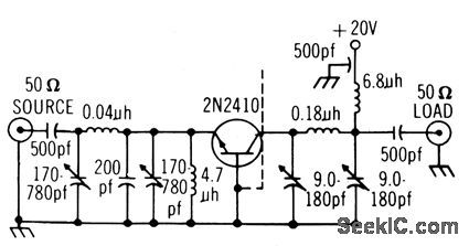
Power output is up to 1 w and collector efficiency above 50% for common-base operation.-Texas Instruments Inc., Solid-State Communications, McGraw-Hill, N.Y., 1966, p 317. (View)
View full Circuit Diagram | Comments | Reading(783)
ADJUSTABLE_BANDWIDTH_AMPLIFIER
Published:2009/7/13 4:35:00 Author:May
Bandwidth can be varied from 190 to 280 kc by varying bias voltage on varicap diodes between 0 and 10 v.Used in frequency-response equalization and other system applications requiring automatically adiustable bandwidth in low-poss circuit.-M. G. Wilson, Low-pass Amplifier with Adiustable Bandwidth, Electronics, 39:11, p 90-91. (View)
View full Circuit Diagram | Comments | Reading(713)
250_MC_POWER_AMPUFIER
Published:2009/7/13 4:33:00 Author:May

Gives good per formance for both small and large signals.-Texas Instruments Inc., Solid-State Communications, McGraw-Hill, N.Y., 1966, p 320. (View)
View full Circuit Diagram | Comments | Reading(652)
CALCULATOR_COUNTS_UP_TO_300_Hz
Published:2009/7/13 4:33:00 Author:May

Logic elements used with MM5736 calculator chip provide self-starting counting action In range from 80 to 300 Hz,Increase In counting rate is obtained by feeding digit output 6 back to digit output 4, to bypass some internal logic of calculator. -M. Watts, Calculator Chip Makes a Counter, National Semiconductor, Santa Clara, CA, 1974, AN-112、p4 (View)
View full Circuit Diagram | Comments | Reading(2098)
FLASH_TRIGGER
Published:2009/7/13 4:33:00 Author:May

Used in instrument designed to trigger up to five individual flash units at equal increments of time that can rangefrom 11 ms to 11s, as required for such assignments as taking sequence photographs of springboard diver in flight. Transistors Tr1, Tr2, and Tr3 form monostable MVBR that is switched to unstable state by negative pulse applied to base of Tr2 by SCR1 when camera shutter contacts FL1 are closed. Timing circuit Tr4-Tr5-Tr6 provides ramp output at A for feeding voltage-operated switches set to trip at different points of ramp waveform as required for triggering flashes in sequence. Article gives all circuits and setup procedure. Regulated 19.5-V supply is required.-R. Lewis, Multi-Flash Trigger Unit, Wireless World, Nov. 1973, p 529-532. (View)
View full Circuit Diagram | Comments | Reading(828)
2_BIT_BINARY
Published:2009/7/13 4:32:00 Author:May

Sections of RS7473 dual flip-flop are connected to form simple counter that counts to three in binary with LEDs, By adding more flip-flop stages, count can be extended to higher values. If OFF LED represents 0 and ON LED is 1, combinations 00, 01, 10, and 11 rep-resent 0, 1, 2, and 3, respectively. Input is restricted to low audio frequency so LED changes can be readily observed during demonstrations. -F. M. Mims, Integrated Circuit Projects, Vol, 6, Radio Shack, Fort Worth, TX, 1977, p23-32. (View)
View full Circuit Diagram | Comments | Reading(662)
CONSTANT_CURRENT_DIODE_AS_COLLECTOR_LOAD
Published:2009/7/13 4:32:00 Author:May

Gain is 45 with 4.7K resistive load, and increases to 750 with CCD as load.Gain-reducing effect of external load paralleling CCD can be eliminated by using emitter.follower to isolate load from collector circuit.-T.K.Hemingway, Applicclfions of the Constant-Current Diode,Electronics, 34:42, p 60-63. (View)
View full Circuit Diagram | Comments | Reading(1347)
TOUCH_SWITCH_2
Published:2009/7/13 4:31:00 Author:May

Small AC signal momentarily introduced by finger contact on touch plate causes voltage at pin 8 of CA3098 dual-input precision level detector to be greater than high reference voltage. This toggles memory flip flop in IC, making voltage high at pin 5. Vottage at pin 7 then increases exponentially to V+ in about 10 s.This 10-sdelay is maximumthat button can betouched; longertouch makes system oscillate between ON and OFF states until finger is removed. Shorter touch energizes load, placing pin 7 at V+. Next touch of plate turns circuit off.-G. J. Granieri, Precision Level Detector IC Simplifies Control Circuit Design, EDN Magazine, Oct. 5, 1975, p 69-72. (View)
View full Circuit Diagram | Comments | Reading(0)
TWO_CHIP_COUNTER
Published:2009/7/13 4:31:00 Author:May

Combination of Na-tional MM5736 calculator chip and DM75492 digit driver for 6-digit LED display is suitable for applications where typical maximum counting rate can be about 100 Hz. Counter is reset manually by closing S1 to clear calculator and closing S2 to enter a 1. Operator now controls start of new count by pressing S,, without need for gating count input. -M. Watts, Calculator Chip Makes a Counter, National Semiconductor, Santa Clara, CA, 1974, AN-112, p 2. (View)
View full Circuit Diagram | Comments | Reading(980)
BAR_GRAPH_DISPLAY_DRIVER_SCALE_SETTING
Published:2009/7/13 4:31:00 Author:May

The figure shows ways of varying the reference with the internal generator of the bar-graph driver chip. (a) and (b) show two obtain full scales of 1 V and 0.5 V, respectively. In (c), the reference adjust and internal reference are used to produce 2 V. (View)
View full Circuit Diagram | Comments | Reading(689)
SELF_DRIVING_COUNTER
Published:2009/7/13 4:29:00 Author:May


UJT relaxation oscillator Q1 supplies series of pulses to input pin 14 of RS7490 decade counter at frequency determined by setting of R2 and value used for C1 Counter feeds corresponding BCD outputs to BCD input pins of RS7447 decoder for conver-sion into 7-segment decimal format for driving Radio Shack 276-052 LED display. Ideal for class-room demonstrations a nd Science Fair exhibits. 6-V battery with 1N914 diode in series can be used in place of 5-V supply. -F. M. Mims, In-tegrated Circuit Projects, Vol. 2, Radio Shack, Fort Worth, TX, 1977, 2nd Ed., p 41-56. (View)
View full Circuit Diagram | Comments | Reading(3670)
CONTACTLESS_KEYBOARD
Published:2009/7/13 4:29:00 Author:May

Touching one of 16 metal pads at inputs of 74150 multiplexor produces corresponding 4-bit BCD output from 74194 shift register. During scanning of multiplexer inputs by counter, output is produced only when finger of operator is on corresponding fingertip-size touch pad. Requires 10-kHz pulse from external source to strobe multiplexer and serve as clock for counter. Duration of clock pulse must be more than 20 ns so untouched pads charge up to threshold voltage but not long enough to let touched pad charge.-D. Cockerell, TTL IC Serves as Touch Keyboard, Electronics, Feb. 20, 1975, p 108-109. (View)
View full Circuit Diagram | Comments | Reading(3053)
| Pages:703/2234 At 20701702703704705706707708709710711712713714715716717718719720Under 20 |
Circuit Categories
power supply circuit
Amplifier Circuit
Basic Circuit
LED and Light Circuit
Sensor Circuit
Signal Processing
Electrical Equipment Circuit
Control Circuit
Remote Control Circuit
A/D-D/A Converter Circuit
Audio Circuit
Measuring and Test Circuit
Communication Circuit
Computer-Related Circuit
555 Circuit
Automotive Circuit
Repairing Circuit