
Circuit Diagram
Index 715
Telephone electronic lock circuit diagram
Published:2011/8/4 5:07:00 Author:Rebekka | Keyword: Telephone electronic lock

Telephone electronic lock uses the key (there is a resistance plug)inserts into the circuit and makes the periodic circuit start to oscillation. And the accuracy of the oscillation frequency can decide whether the telephone call can be opened and the receive of the external calls will not be affected. This can make sure that only the man who owns the key can uses the telephone. The circuit of the telephone electronic lock is shown as above. It is mainly composed of frequency key unlock circuit, ringing signal identifyinglock circuit, self-locking lock circuit and other components.
(View)
View full Circuit Diagram | Comments | Reading(1144)
QUAD_BLOCK
Published:2009/7/16 3:55:00 Author:Jessie
With appropriate interconnections of external terminals, can be used either as binary counter, monostable mvbr, Schmitt trigger, or selector. Although original design uses encapsulated construction, can readily be adapted for integrated circuit production techniques. Requires 10 ma for all applications, and gives output pulses with 0.1 microsec rise time and up to 0.4 microsec fall time.-F. K. Luteran, Four-Way Quad Circuit Building Block, EEE, 10:6, p 66-67. (View)
View full Circuit Diagram | Comments | Reading(775)
3_kV_SUPPLΥ
Published:2009/7/13 3:15:00 Author:May

Circuit uses full-wave bridge rectifier D2-D5, with each diode stack constructed from two 1000-PIV 2.5-A diodes in series. Each diode pair is shunted by 470K 1-W resistorand 0.01-μF 1000-V disk capacitor C2-C11 are 500 μF at 450 VDC. Capacitor combination thus gives equivalent of 50 μF for filter, rated 4500 V. When using 500-μA movement for output voltmeter, R5 should be ten 1-megohm resistors in series. Thyrector TY1 is GE 6R52OSP4B4. T1 has 2200-V secondary rated 500 mA. K1 is 24-V relay. Article covers construction and stresses safety precautions.-E.H. Hartz, 3000 VDC Supply, 73 Magazine, July 1974, p 69-72. (View)
View full Circuit Diagram | Comments | Reading(971)
HEADLIGHT_DIMMER_1
Published:2009/7/16 3:55:00 Author:Jessie
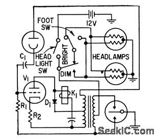
Automatically switches from high to low beam when oncoming head-light strikes photocell. Driver may dim lights manually at any time and leave them dim. When lights have been dimmed automatically, momentary reduction of light on photo-cell will not cause return to high beam.-W.E. Bushor, Electronics and the American Auto-mobile, Electronics, 31:47, p 73-79.
(View)
View full Circuit Diagram | Comments | Reading(599)
TV_GAME_CONTROL
Published:2009/7/13 3:15:00 Author:May

Developed for use in game in which first person to recognize musical tune places finger on touch plate to energize his lamp. Action stops cassette player andlocks out touch plates of other players. After 5-s delay, lockout is disabled so different player can have try at correct answer if first is wrong. After additional 5-s delay, relay is deenergized and music resumes. Additional reset switch is provided to reactivate all touch plates independently of delay. Supply is 12 V, and lamps are 12 V.-J. Sandler, Name That Tune, Modern Electronics, Dec. 1978, p 66 and 69-70. (View)
View full Circuit Diagram | Comments | Reading(725)
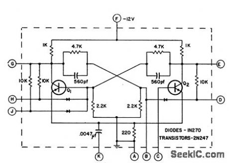
PARALLEL_PNP_BASIC_LOGlC
Published:2009/7/16 3:55:00 Author:Jessie
Serves as or gate for normally open switches and as and gate for normally closed switches. Provides phase inversion of input.-Texas Instruments Inc., Transistor Circuit Design, McGraw-Hill, N.Y., 1963, p 388. (View)
View full Circuit Diagram | Comments | Reading(575)
160_METERS_TO_l0_METERS
Published:2009/7/16 3:55:00 Author:Jessie
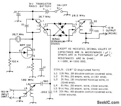
Simple converter adds 160-meter band capability to older CW or AM receiver. Passive mixer is adequate. High output frequency eliminates IF feedthrough and image signals. Crystal oscillates on third over-tone and feeds directly into mixer. -A. Bloom, A Simple 160-Meter Converter, QST, Feb. 1975, p46. (View)
View full Circuit Diagram | Comments | Reading(1283)
GROUNDED_LINE_CABLE_DRIVER
Published:2009/7/13 3:14:00 Author:May

Twisted 100 ohm d-c coupled tranmission line solves ground-differential problem between driving and receiving subsystems up to 120 feet apart, while eliminating costly transformer coupling. Holding line excursion to 1.5V minimizes capacitive crosstalk. Up to four receivers can be used on one line.-R. C.Garavalia.Transimission lines Couple Multiple-Driver Receivers.Electronics.39:16,p121-122. (View)
View full Circuit Diagram | Comments | Reading(569)
TRANSFORMERLESS_DC_TO_DC_CONVERTER
Published:2009/7/13 3:14:00 Author:May
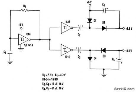
This configuration should prove handy in situations in which dual-polarity supplies are needed for a few devices on a board that has only one +5-V supply. The circuit doesn't need any dc-to-dc converter ICs, nor does it require any transformers or inductors. Three Schmitt-trigger inverters, such as the 7414, form the heart of the circuit (see the ftgure). One inverter is configured as a high-frequency astable multivil)rator employing a single resistor and a capacitor. For the RC values shown, the frequency of the astable output is around 100 kHz. The frequency of the oscillation is given by f=1/T, where T=R1C1 ln[1-VCC/VLT)/(1-VCC/VUT)] and R1 and C1 are the timing components of the astable multivibrator, VCC is the supply voltage, and VLT and VUT are the lower trip point and upper trip point of the Schmitt trigger. The astable multivibrator's output drives a pair of inverters that, in turn, drive a pair of diode-capacitor voltage-doubler circuits. The outputs of the diode-capacitor circuits are around 8.5 V with the polarities shown. Diodes D1 to D4 should be fast-switching types, like the 1N914 or 1N4148. As a result, the circuit can generate ±8.5 V from a single +5-V sup-ply making it useful in many applications. (View)
View full Circuit Diagram | Comments | Reading(1369)
PARALLEL_NPN_BASIC_LOGIC
Published:2009/7/16 3:54:00 Author:Jessie

Serves as or gate for normally open switches and as and gate for normally closed switches. Provides phase inversion of input.-Texas Instruments Inc., Transistor Circuit Design, McGraw-Hill, N.Y., 1963, p 388. (View)
View full Circuit Diagram | Comments | Reading(653)
CHOPPER_DRIVING_SIGNAL_GENERATOR
Published:2009/7/16 3:53:00 Author:Jessie

Dual mos fet and Fairchild 709 IC null amplifier are here used with 1-kc fee useable mvbr to develop the large voltage swings required to drive chopper of linear IC tester.-J. N. Giles, How to Measure Linear. IC Performance, EEE, 14:8, p 62-68 and 161 (View)
View full Circuit Diagram | Comments | Reading(690)
PROXIMITY_SWITCH
Published:2009/7/13 3:14:00 Author:May

Hand brought near sensor plate induces 60-Hz power-line hum in section of quad two-input NOR gate. Hum is squared bygateand used to trip section of 4013 connected as retriggerable mono MVBR. Output of mono is clean from instant of first proximity until several milliseconds after moving hand away. Sensitivity depends on size of metal plate and on number of permissible false alarms from other noise sources nearby.-D. Lancaster, CMOS Cookbook, Howard W. Sams, Indianapolis, IN, 1977, p 278-282. (View)
View full Circuit Diagram | Comments | Reading(0)
120_W300_V_D_C_AUTO_CONVERTER
Published:2009/7/16 3:53:00 Author:Jessie
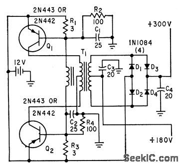
For 12-v auto systems. Develops square-wave voltage at 200 cps, for conversion to 300 v d-c by silicon-diode bridge rectifier. Each switching transistor requires T-inch-square sheet of 1/8th-inch aluminum as heat sink.-W. E. Bushor,Electronics and the American Automobile, Electronics, 31:47, p 73-79. (View)
View full Circuit Diagram | Comments | Reading(704)
ADC_CONTROLLING_DIGITAL_POTENTIOMETER
Published:2009/7/13 3:09:00 Author:May

This design was created to control a DS1267 digital potentiometer with an analog signal. The DS1267 is a dual-pot chip, but this design will enable control of only one section. Here, the analog-to-digital converter (ADC) used is an ADC0833 8-bit serial I/O converter with a four-channel multi-plexer. The analog input to channel 3 of the ADC is employed. The timing diagram illustrates the operation of the circuit. A negative start pulse on the chip select of the ADC starts the sequence (the pulse must stay low for at least 14 clock pulses or until the ADC's SAR Status line comes high). The next five clock pulses perform various housekeeping in the ADC, The Data 0ut line comes out of tristate on the negative edge of the fifth pulse, and the SAR Status line comes high to signal a conversion in progress. The first bit on the Data Out line is a leading zero for one clock period. Data is clocked into the DS1267 on the positive edge of the clock pulse. The input format for the DS1267 requires that the first bit determine the stack select (used in the DS1267 when the two pots are com-bined) and the following 8 bits provide data. Following transmission of these 9 bits, the SAR Status line goes high, disabling further input to the DSl267 (the ADC0833's output format continues trans-mission of 8 more bits of the conversion in reverse order, but the DS1267 ignores these). Input range for the ADC is 0 to 5 V. Pin 1 of the DS1267 is shown tied to ground (for pot connections referenced to ground; however, -SVcan be used to provide a range of 15 to -5 V on the pot). (View)
View full Circuit Diagram | Comments | Reading(3300)
DIGIT_LINE_DRIVER
Published:2009/7/16 3:53:00 Author:Jessie
Uses diode steering to increase speed of memory.-A.Melmed, R,Shevlin, and W. Orvedahl, Diode Steering Increases Speed of Magnetic Memories, Electronics,34:37,p 68-70. (View)
View full Circuit Diagram | Comments | Reading(523)
LOGIC_SWITCH
Published:2009/7/13 3:09:00 Author:May

Can be used with batterypowered circuits because CMOS touch switch does not require body pickup of AC Iine hum for switchina action. Schmitt trigger IC1 forms 100 kHz oscillator. IC2a amplifies oscillator output and charges C1 through diode. When sensor is touched, oscillator output is severely attenuated, making C1 discharge and thereby changing output state of level detector IC2b. Sensor is 1-inch-square of double-sided printed-circuit board with lower side divided into two equal sections.-N. Sunderland, C.M.O.S. Touch Switch, Wireless World, May 1978, p 69. (View)
View full Circuit Diagram | Comments | Reading(1003)
VOICE_OPERATED_MACHINE_CONTROL
Published:2009/7/13 3:08:00 Author:May
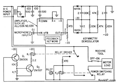
Circuit rejects ambient noise or normal speech but responds to sharply spoken commands during emergency, to open motor circuit of machine tool. Asymmetry demodulator rejects symmetrical noise while accepting speech vowels having strong asymmetry.-W.C.Dersch.Speech Operates Safety Switch.Electronics.36:25,p78-82 (View)
View full Circuit Diagram | Comments | Reading(568)
CURRENT_LIMITING_A_SERIES_REGULATOR
Published:2009/7/13 3:07:00 Author:May

If the current limitation of the series-pass transistor is exceeded, transistor Q1 could be damaged or destroyed. This can be prevented with the addition of a current-limiting transistor, as shown in the figure. When the current through Q1 becomes high enough, the voltage drop across R2 becomes high enough to forward-bias transistor Q2. When Q2 starts to conduct, its internal resistance decreases. When this occurs, the forward bias of Q1 is fixed, and its output is a constant current. The current-limiting transistor and resistor in the figure protect the pass transistor and rectifier diodes if the load terminals are accidentally short-circuited. However, the addition of transistor Q2 increases the already high power dissipation in pass transistor Q1 when the load demand is high. (View)
View full Circuit Diagram | Comments | Reading(627)
TOUCH_PLATE_RELAY
Published:2009/7/13 3:06:00 Author:May

When 2-inch diameter disk of sheet metal or foil is firmly touched with finger, stray noise picked up by body and coupled into 10-megohm gate circuit of FET is sufficient to boost drain current to about 1.7 mA and close relay. Delayed dropout can be obtained by placing capacitor in parallel with relay coil; delay is about 0.8 s per 1000 μF of parallel capacitance.-R. P. Tumer, FET Circuits, Howard W. Sams, lndianapolis, IN, 1977, 2nd Ed., p 104-105. (View)
View full Circuit Diagram | Comments | Reading(1048)
AUDIO_AMPLIFIER
Published:2009/7/13 3:06:00 Author:May
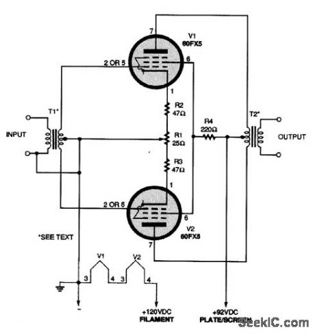
Some hobbyists still prefer to use older vacuum tube technology. A push-pull audio amplifier using a pair of 60FX5 tubes is shown in the figure. T1 is a 1:3 audio interstage, while T2 is a universal output transformer of about 5000 Ω to voice coil (4 or 8 Ω) impedance. (View)
View full Circuit Diagram | Comments | Reading(0)
| Pages:715/2234 At 20701702703704705706707708709710711712713714715716717718719720Under 20 |
Circuit Categories
power supply circuit
Amplifier Circuit
Basic Circuit
LED and Light Circuit
Sensor Circuit
Signal Processing
Electrical Equipment Circuit
Control Circuit
Remote Control Circuit
A/D-D/A Converter Circuit
Audio Circuit
Measuring and Test Circuit
Communication Circuit
Computer-Related Circuit
555 Circuit
Automotive Circuit
Repairing Circuit