Amplifier Circuit
LOW_NOISE_9_MHz_AGC_CONTROLLED_AMPLIFIER
Published:2009/7/13 2:44:00 Author:May | From:SeekIC


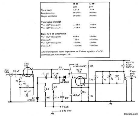
The circuit diagram of the 9-MHz amplifier is given. Note that the AGC amplifier must be capable of sinking the current through D1 at 0 V (i.e., maximum gain). The warning to keep leads short in the drain circuit of the second U310 FET arises from experience in which the initial IP3 measurements proved to be poor because of this stage's oscillating around 400 MHz.Component notes: The two U310s are Siliconix low-noise JFETs. C1 is an 82-pF ceramic, C2 is a 60-pF ceramic trimmer (Cirkit), and all other capacitors are monolithic ceramic (RS components). Resistors are l/8 Wmetalfilm (RS components). D1 and D2 are HP3081 PIN diodes (Farnell). T1 is 1518 turns of 0.224-mm diameter Bicelflux enamel on Fairite Balun core 28-43002402 (Cirkit). T2 (primary) is 2.81 μH, 31 turns of 0.314-mm Bicelflux enamel on Micrometals toroid 737-6 (Cirkit). T2 (secondary) is (1) for 16-dB gain, 3 turns, Rx 6k2; (2) for 13-dB gain, 4 turns, Rx 3k9. Note that (1) and (2) could be relay switched for use with an SSB or CW filter (loss 10 dB or 3 dB). L1, L2, and L3 have 7 turns of 9.314-mm enamel on balun core 28-43002402 (Cirkit).
Reprinted Url Of This Article:
http://www.seekic.com/circuit_diagram/Amplifier_Circuit/LOW_NOISE_9_MHz_AGC_CONTROLLED_AMPLIFIER.html
Print this Page | Comments | Reading(3)

Article Categories
power supply circuit
Amplifier Circuit
Basic Circuit
LED and Light Circuit
Sensor Circuit
Signal Processing
Electrical Equipment Circuit
Control Circuit
Remote Control Circuit
A/D-D/A Converter Circuit
Audio Circuit
Measuring and Test Circuit
Communication Circuit
Computer-Related Circuit
555 Circuit
Automotive Circuit
Repairing Circuit
Code: