
Circuit Diagram
Index 722
PRODUCT_DETECTOR
Published:2009/7/16 5:00:00 Author:Jessie

Excellent isolation is provided by dual-gate MOSFET. Used for demodulating SSB or CW signals. Input resonant circuit is tuned to IF value. High-frequency components of signal are filtered out by drain output circuit. RC low-pass filter passes voice frequencies to succeeding audio amplifier.-E. Noll, MOSFET Circuits, Ham Radio, Feb.1975, p50-57. (View)
View full Circuit Diagram | Comments | Reading(0)
2_METER_VMOS_ADDITIVE_MIXER
Published:2009/7/16 4:59:00 Author:Jessie

Single-ended circuit for amateur band can deliver 0.5 W of power to IF amplifier while providing conversion gain of 18 dB and compression level of 10 dBm. Noise figure is 5.2 dB. Traps in both signal and noise feeds to Siliconix VMP-4 power transistor prevent radiation of unwanted signals. - E. Oxner, Will VMOS Power Transistors Replace Bipolars in HF Systems ? , EDN Magazine, June 20, 1977, p 71-75. (View)
View full Circuit Diagram | Comments | Reading(726)
EPIIAXIAL_NOR_GATE
Published:2009/7/16 4:59:00 Author:Jessie

Operates at up to 8Mc from -55°C to+150°C.-D,Hall Using Epitaxial Transistors in Switching and R-F Circuits. Electronics, 34:13, p 52-53. (View)
View full Circuit Diagram | Comments | Reading(636)
MONOSTABLE_PULSE_FORMER
Published:2009/7/16 4:58:00 Author:Jessie

Output stage of driver serves also as first stage of monostable multivibrator, with saving in components. Here Q2 is output of Schmitt trigger and first stage of monostable mvbr Q2-Q1. –R. L. Paul and A. S. Ottenstein, Eliminating the First State of a Monostable Multivibrator, Electronics, 35:36, p 54-55. (View)
View full Circuit Diagram | Comments | Reading(798)
RESISTOR_TRANSISTOR_NOR_GATE
Published:2009/7/16 4:58:00 Author:Jessie

Circuit is basic building block of binary full adder for high speed encoding Transistor is 2N1499.-S. C. Chao, High Speed Encoding with Resistor-Transistor-Logic Circuits, Electronics, 35-6.p 48-51. (View)
View full Circuit Diagram | Comments | Reading(680)
SINGLE_TRANSISTOR__ONE_SHOT
Published:2009/7/16 4:57:00 Author:Jessie

Requires fewer components and gives higher reliability. –T. F. One-Transistor Single-Shot, Electronics, 34:16, p 66. (View)
View full Circuit Diagram | Comments | Reading(1198)
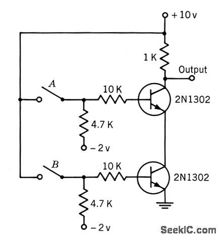
NEON_WITH_PNP_EXCLUSIVE_OR_LOGIC
Published:2009/7/16 4:57:00 Author:Jessie

Neon lamp glows when inputs are in agreement. Indicator will follow only one control level if other input is at fixed voltage such as logic 0; lamp will then turn off whenever control input is at logic 1. Similarly, if fixed voltage is logic 1, lamp will turn off when control input is at logic 0.-Exclusive OR Uses One Transistor, Electronic Circuit Design Handbook, Mactier Pub. Corp., N.Y., 1965, p 213. (View)
View full Circuit Diagram | Comments | Reading(693)
DELAYED_OUTPUT_PULSE
Published:2009/7/16 4:56:00 Author:Jessie

Only three transistors are required to generate output rectangular pulse that is delayed a predetermined time after arrival of input pulse. Delay time is determined by C1, R3, and R4, and is about 10 microsec for values shown. Output pulse width is also about 10 microsec. -T. R. Ferrara, Delayed Pulse Generator, EEE, 13:10, p 71 (View)
View full Circuit Diagram | Comments | Reading(645)
NPN_AND_GATE
Published:2009/7/16 4:55:00 Author:Jessie


Two diodes act as conventional and gate with transistor and its collector supply, using few components. Intended for 0 and -6 V logic.-Exclusive OR Uses One Transistor, Electronic Circuit Design Handbook, Mactier Pub. Corp., N.Y., 1965, p 213. (View)
View full Circuit Diagram | Comments | Reading(760)
CALIBRATED_MILLIMICROSECOND_PULSER
Published:2009/7/16 4:55:00 Author:Jessie

Uses coaxial discharge line to produce precise short pulses on keyed single-shot basis or of constant repetition rate. Works into 50-ohm load.-E. J. Martin, Jr., Calibrated Source of Millimicro second Pulses, Electronics, 32:16, p 56-57. (View)
View full Circuit Diagram | Comments | Reading(658)
DOUBLE_NOR_GATE
Published:2009/7/16 4:55:00 Author:Jessie


Pulse repetition rate is 1Mc, fanin is 3, and fanout is up to 6, with 30-mw dissipation for 7-v supply.-Double NOR Gate for Dense Packaging, Electronics, 36:12, p 100. (View)
View full Circuit Diagram | Comments | Reading(727)
PNP_EXCLUSIVE_OR_LOGIC
Published:2009/7/16 4:54:00 Author:Jessie

For use with0 (ground) and -6 v logic system. Can be adapted readily to most other logic levels. Produces logic 1 when inputs disagree.-Exclusive OR Uses One Transistor, Electronic Circuit Design Handbook, Mactier Pub. corp,N.Y.1965,p213. (View)
View full Circuit Diagram | Comments | Reading(748)
20_METER_DIRECT_CONVERSION_CW_SSB
Published:2009/7/16 4:53:00 Author:Jessie
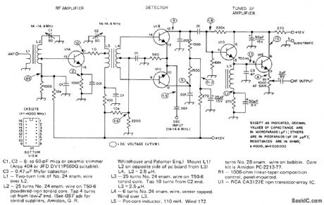
Simple direct-conversion or synchrodyne receiver uses RCA CA3127E five-transistor array. Product detector follows 14-MHz RF stage. Low drain makes receiver ideal for battery operation, but circuit has no AGC. AF output will drive headphones adequately for strong 20-meter signals, but not loudspeaker. Local-oscillator energy at 14-14.4 MHz for product detector at 1.5-2 VRMS must be furnished by external BFO.-D. DeMaw, Understanding Linear ICs, QST Jan. 1977, p 11-15. (View)
View full Circuit Diagram | Comments | Reading(2074)
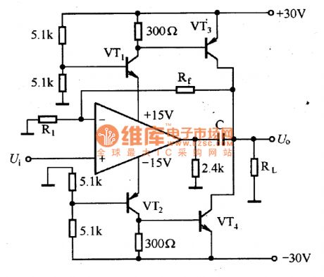
Improving load capacity circuit diagram
Published:2011/7/15 10:01:00 Author:Nancy | Keyword: load capacity
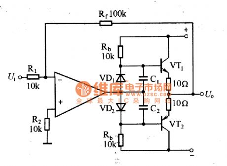
The load capacity of the general integrated operational amplifier load ability is weak, it only allows for dozens of mV power consumption, the maximum output current is also only 10 mA. So, when need large load voltage or current, you need add circuit with extended function at its output pin.
The circuit shown as figure a is a circuit using complementary push-pull output to expand current. When Ui = 0, Uo = 0, the current flows through the base loop of Rb, VD1, VD2 and VT1,VT2 and it provides bias current to VT1 and VT2, which makes it work in A B amplification state and reduce crossover distortion. The weakness of the circuit is that it can't raise voltage range.
The circuit shown as figure b is a circuit which can expand current and voltage range. (View)
View full Circuit Diagram | Comments | Reading(670)
1930~1990MHz narrowband linear amplification circuit composed of RF2320
Published:2011/8/4 5:00:00 Author:May | Keyword: narrowband linear amplification
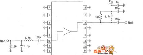
The picture shows 1930~1990MHz narrowband linear amplification circuit composed of RF2320. Radio-frequency signal (RF) is input by pin 6. Then it is output by pin 14 after passing amplifier. Pin 6 is direct coupled with internal amplifier. So it adds a blocking coupling capacitor. Normally, the gate voltage of input end is 0V. But the gate voltage will be enlarged when extent bias enlarges, and current will be increased at the same time. But it can not improve the linearity of amplifier. Pin 14 provides output and internal bias. There is no blocking coupling capacitor in the chip, but this pin has DC voltage. So it adopts 22pF capacitor to use as blocking capacitor. In order to get thelargest output power and efficiency, output matching network can make output impedance of amplifier match with it.
(View)
View full Circuit Diagram | Comments | Reading(694)
SERIES_NPN_BASIC_LOGIC
Published:2009/7/16 4:53:00 Author:Jessie
Serves as and gate for normally open switches, and as or gate for normally dosed switches. Provides phase inversion of input.-Texas Instruments Inc., Transistor Circuit Design, McGraw-Hill, N.Y., 1963, p 388. (View)
View full Circuit Diagram | Comments | Reading(724)
LED_PEAK_INDICATOR
Published:2009/7/16 4:53:00 Author:Jessie

The voltage divider consisting of resistor R6 and 2.5-V precision voltage reference IC2 forms a precision voltage reference whose voltage is divided in half at the junction of resistors R7 and R8.This places a reference voltage of 1.25V at the comparator noninverting input. Whenever the inverting input voltage exceeds the reference voltage, the output will be connected to ground internally, and LED1 will light. With the input of this circuit connected to the output of the averager circuit, the LED will flash on whenever the audio input exceeds the level set with gain potentiometer R2. Adjust R2 by applying a maximum level signal to the input of the averager, and then reduce the level slightly to allow for headroom. With the input level now set, adjust R2 until the peak LED just turns on. (View)
View full Circuit Diagram | Comments | Reading(1406)
14_30_MHz_PRESELECTOR
Published:2009/7/16 4:51:00 Author:Jessie
Simple self-powered preselector using FET improves overall noise figure of shortwave receiver along with sensitivity in 14-30 MHz portion of HF band. Also helps reduce cross-modulation from strong out-of-band shortwave broadcast stations. C1 and C2 are 50-500 pF Miller 160B. L1 is 10 turns No. 22 on 750-10 Micrometals core with 1-turn link. L2 is 10 turns No. 22 with center tap and 2-turn link on 750-10 core, Q1 is MPF102, HEP-802, or HEP-F0015. D1 and D2 are 1N4002 or HEP-R0051.-H. Olson, The S38 Is Not Dead!, 73 Magazine, Nov. 1976, p 88-89. (View)
View full Circuit Diagram | Comments | Reading(1521)
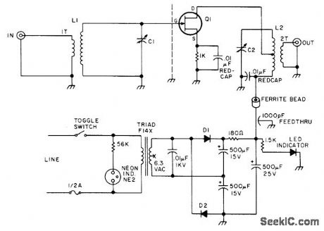
3_kV_FOR_CRO
Published:2009/7/13 2:38:00 Author:May

Circuit also provides 1-kV negative supply at 2 mA, as required for cathoderay tube of oscilloscope. Positive supply furnishes 50 μA at 3 kV. Design uses transistor inverter operating at about 20 kHz to simplify filtering. Tr82 and Tr83 form current-switched class D oscillator producing sine waves at high efficiency. Current multiplication is provided by Tr80 and Tr81 for 709 IC opamp.-C.M. Little,A 50 MHz Oscilloscope, Wireless World, July 1975,p 319-322. (View)
View full Circuit Diagram | Comments | Reading(2191)
VARIABLE_PULSE_WIDTH_GENERATOR
Published:2009/7/16 4:51:00 Author:Jessie
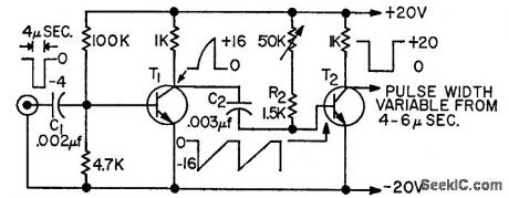
Converts fixed negative pulse-width input to variable and stable pulse width. Will accept positive inputs if T1 and T2 are changed from 2N1308 to 2N1309 and collector voltages reversed. Will operate at repetition rates from 30 cps to 2 Mc, with pulse widths from 600 microsec to 100 nsec. With values shown, maximum duty cycle is 92% with 63-microsec input rep rate.-H. D. Flagle, High-Duty-Cycle Pulse-Width Genera. tor, FEE, 11:8, p 27-28. (View)
View full Circuit Diagram | Comments | Reading(784)
| Pages:722/2234 At 20721722723724725726727728729730731732733734735736737738739740Under 20 |
Circuit Categories
power supply circuit
Amplifier Circuit
Basic Circuit
LED and Light Circuit
Sensor Circuit
Signal Processing
Electrical Equipment Circuit
Control Circuit
Remote Control Circuit
A/D-D/A Converter Circuit
Audio Circuit
Measuring and Test Circuit
Communication Circuit
Computer-Related Circuit
555 Circuit
Automotive Circuit
Repairing Circuit