Amplifier Circuit
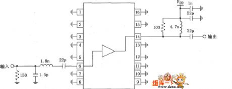
1930~1990MHz narrowband linear amplification circuit composed of RF2320
Published:2011/8/4 5:00:00 Author:May | Keyword: narrowband linear amplification | From:SeekIC

The picture shows 1930~1990MHz narrowband linear amplification circuit composed of RF2320. Radio-frequency signal (RF) is input by pin 6. Then it is output by pin 14 after passing amplifier. Pin 6 is direct coupled with internal amplifier. So it adds a blocking coupling capacitor. Normally, the gate voltage of input end is 0V. But the gate voltage will be enlarged when extent bias enlarges, and current will be increased at the same time. But it can not improve the linearity of amplifier. Pin 14 provides output and internal bias. There is no blocking coupling capacitor in the chip, but this pin has DC voltage. So it adopts 22pF capacitor to use as blocking capacitor. In order to get thelargest output power and efficiency, output matching network can make output impedance of amplifier match with it.
Reprinted Url Of This Article:
http://www.seekic.com/circuit_diagram/Amplifier_Circuit/1930~1990MHz_narrowband_linear_amplification_circuit_composed_of_RF2320.html
Print this Page | Comments | Reading(3)

Article Categories
power supply circuit
Amplifier Circuit
Basic Circuit
LED and Light Circuit
Sensor Circuit
Signal Processing
Electrical Equipment Circuit
Control Circuit
Remote Control Circuit
A/D-D/A Converter Circuit
Audio Circuit
Measuring and Test Circuit
Communication Circuit
Computer-Related Circuit
555 Circuit
Automotive Circuit
Repairing Circuit
Code: