
Circuit Diagram
Index 741
HIGH_VOLTAGE_PULSE_SUPPLY
Published:2009/7/16 21:02:00 Author:Jessie

This high-voltage pulse supply will generate pulses up to 30 kV. Q1 and Q2 form a multivibrator in conjunction with peripheral components R1 through R6 and C1, C2, C3, C5, C6, and D2. R9 adjusts the pulse repetition rate. R2 should be selected to limit the maximum repetition rate to 20 Hz. I1 is a type 1156 lamp used as a current limiter. R9 can be left out and R2 selected to produce a fixed rate, if desired.Try about 1 MΩ as a start.Q3 serves as a power amplifier and switch to drive T1 (an automotive ignition coil). NE1 is used as a pulse indicator and indicates circuit operation. Because this circuit can develop up to 30 kV, suitable construction techniques and safety precautions should be observed. (View)
View full Circuit Diagram | Comments | Reading(1026)
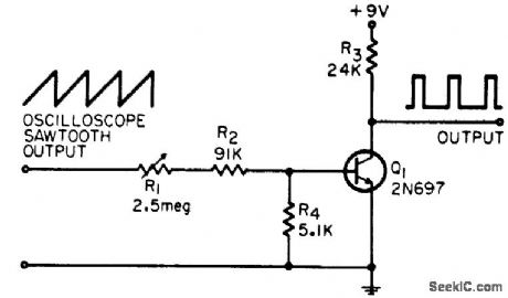
STROBE_PULSE_GENERATOR
Published:2009/7/16 21:02:00 Author:Jessie
Constant-amplitude sawtooth from timebase of display unit is fed to one control grid of Schmitt trigger V1, whose output triggers one-shot mvbr to produce gating pulse 0.1 millisec wide that also identifies strobed channel on crt by brightening trace c-d that point.-A. Potton, Telemetry System for Testing Automobiles,Electronics, 33:43, p 57-59. (View)
View full Circuit Diagram | Comments | Reading(756)
SIMPLE_25_MHz_COUNTER
Published:2009/7/12 22:56:00 Author:May

An Intersil ICM7224 is used to drive an LCD003 four-digit LCD display unit. Three inputs are provided, which add signal conditioning, either gain, rectification, or unbuffered input. A Statek PXO-1000 1-MHz clock is used as a frequency reference. S2 selects gate time and hence range, with LED1, LED2, and LED3, indicating Hz, kHz, or MHz, respectively. (View)
View full Circuit Diagram | Comments | Reading(2237)
VARIABLE_WIDTH_AND_VARIABLE_PRR
Published:2009/7/16 21:01:00 Author:Jessie
Gives wide range of control over pulse width and pulse repetition rate, while maintaining synchronization with oscillosope. Can be con strutted with banana plugs for sawtooth output jacks of scope.-R. G. Rakes, Simple Variable Width, PRR Pulse Generator, EEE, 13:11, p 45-46. (View)
View full Circuit Diagram | Comments | Reading(743)
±9_V
Published:2009/7/16 21:01:00 Author:Jessie

Developed for use with demodulator of teleprinter. Regulation is provided by zeners. -I. Schwartz, An RTTY Primer,CQ, Feb.1978, p 31-36. (View)
View full Circuit Diagram | Comments | Reading(867)
10000_V_STANDARD
Published:2009/7/16 21:01:00 Author:Jessie

The heart of the voltage standard is the LT1027BCH voltage reference IC, IC2, manufactured by Linear Technology Corp. It sports a temperature coefficient of two parts per million per degree Celsius (2 PPM/℃), and it comes pretrimmed within ±0.05 percent. Provision for optional trim circuitry is included on the board; however, it requires an additional resistor-selection step. To eliminate sensitivity to input-voltage variations, the incoming supply is regulated at 15 Vdc. This is accomplished with a conventional LM340T15 voltage regulator, which powers both the reference IC and the output amplifier. The LT1050 amplifier doubles the 5-V output of the LT1027 to the desired 10 Vdc. It is chopper-stabilized, providing far lower drift than a conventional op amp. Noise filtering is provided by the 0.47-μF capacitor across the feedback resistor. Note that the LT1050 does not have the out-put drive of a bipolar device-thus, the slightly higher than normal feedback resistors. You should not try to use the voltage standard with loads below 10 kΩ. The 0.47-μF/49.9-Ω output network improves stability when cables and capacitive loads are driven. (View)
View full Circuit Diagram | Comments | Reading(1107)
AMPLIFIER_FOR_MARKER_GENERATOR
Published:2009/7/16 21:00:00 Author:Jessie

Triode V2A amplifies brightening pulse generated by marker circuit, and feeds amplified pulse to V2B for mixing with fixed or variable external marker pulse so both are applied to Z-axis of scope.-D. J. Odorizzi, Z-Axis Marker Generator for Bandpass Circuit Alignment, Electronics, 33:26, p 108-110. (View)
View full Circuit Diagram | Comments | Reading(834)
COLD_CATHODE_FLUORESCENT_LAMP_SUPPLY
Published:2009/7/16 21:00:00 Author:Jessie

For back-lit LCD displays,this supply will drive a lamp. LT1072 drives Q1 and Q2,and a slne waveappears across C1. L1 is a transformer that steps up this voltage to about 1 400 V D1 and D2 detect lampcurrent and form a feedback loop to the LT1072 to control lamp brightness. (View)
View full Circuit Diagram | Comments | Reading(906)
40_W_120_Vac_INVERTER
Published:2009/7/16 20:59:00 Author:Jessie

This inverter uses a 12.6-V to 120-V transformer to deliver a quasi-sine wave that has the same rms and peak voltage as a pure sine wave. Q1 to Q6 must be heatsinked. A 1.5 x4 aluminum heatsd was used on the prototype. The transformer should be a 3-A unit. The circuit uses feedback to help regulate the output voltage to 120 Vac. Notice that the output frequency is 75 Hz to avoid saturating the core of T1. (View)
View full Circuit Diagram | Comments | Reading(4841)
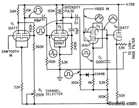
BEAM_INTENSITY_CONTROL
Published:2009/7/16 20:59:00 Author:Jessie

Used to provide two different intensities for symbols on crt.-A. E. Popodi, Reliable Repertoire Of Display Circuits, Electronics, 38:2, p 60-66. (View)
View full Circuit Diagram | Comments | Reading(644)
Timing circuit formed by PUT
Published:2011/8/2 19:44:00 Author:Nancy | Keyword: Timing circuit, PUT
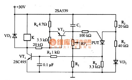
Figure 1 is the timing circuit formed by PUT. It is a 0.5s一lmin time variable timing circuit composed by PUT. The anode-cathode of PUT is offset by the voltage division of fixed resistors R2 and R3, the timing is decided by the capacitor C1 and resistor (R(RP1)十R1) connected to the gate. The base current of the drive transistor VT1 of the relay K is decided by the R2, R4 and R5, it is not relevant to the timing setting resistor for the PUT conduction. The electric charge of capacitor C1 discharges through VT2 and R6, the diode VD1 used to compensate the temperature characteristic of PUT. (View)
View full Circuit Diagram | Comments | Reading(675)
PORTABLE_CRO_UNBLANKING_AMPLIFIER
Published:2009/7/16 20:58:00 Author:Jessie
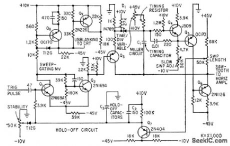
Supplies signal to turn on crt during sweep,Hold-off circuit insures that trace starts from same point on every sweep.-O. Svehaug and J.R. Kobbe,Battery-Operated Transistor Oscilloscope, Electronics, 33:12, p 80-83. (View)
View full Circuit Diagram | Comments | Reading(735)
LOW_COST_SQUARE_WAVES
Published:2009/7/16 20:57:00 Author:Jessie

Conversion circuit coupled to sine-wave audio oscillator gives square wcnre generator at half usual cost. Will shape sine waves upto 3 Mc before trailing edges of square-wave output begin to deteriorate. Can be triggered by input signals from 0.2 to 10 v. Positive input turns on D1 and Q1, driving amplitude-limiting pair Q2-D2 into conductionto square up waveform. Lower half of circuit generates negative square pulse in negative manner.-R. S. Selleck, Converting Audio Oscillators to Square-Wave Generators, Electronics, 39:16, p 123. (View)
View full Circuit Diagram | Comments | Reading(1113)
3_A_SWITCHING_REGULATOR
Published:2009/7/16 20:57:00 Author:Jessie

This switching regulator uses an LM317 and a pnp switching transistor of 3-to 5-A rating. L1 is wound on a commercially available core. (View)
View full Circuit Diagram | Comments | Reading(1279)
GELECTRONIC_DESIGN
Published:2009/7/16 20:56:00 Author:Jessie


Using a charge pump and oscillator, this circuit uses a 7-kHz oscillator. When the clock is high, C and D are on, grounding the positive side of C1 and making negative voltage available at the VSS terminal of U2.With C= C1 + C2, the p-p output ripple is:
Converter output impedance is about 100Ω and maximum current is 10 mA dc. (View)
View full Circuit Diagram | Comments | Reading(709)
STEP_UP_SWITCHINC_IC_INVERTER
Published:2009/7/16 20:56:00 Author:Jessie

A popular step-up switching IC can be made to supply a negative voltage. The MAX641BCPA is a boost converter intended for use with 3-V batteries. To get the 641 to function as an inverter, some of its pin functions must be altered. Pin 1 is used as the voltage-feedback input, and pin 2 is used as the overvoltage-detector output. When the voltage on pin 1 falls below + 1.31 V, pin 2 becomes a low-impedance path to ground. This will force Q1 to cut off and allow the voltage on pin 7 to rise. When the voltage on pin 7 exceeds +1.31 V, the internal oscillator shuts off. At this point, the output voltage is equal to or less than the set level. When C1 discharges to a point where the voltage on pin 1 rises above +1.31 V, pin 2 will change to a high impedance, allowing Q1 to saturate and pull pin 7 below +1.31 V. This causes the internal oscillator to turn on. Pin 4, the output of the internal oscillator, will pump C1 negative while the oscillator is running. For the values shown in the figure, the adjustable output voltage range is approximately -4 to -13 V. The magnitude of the drivable load depends on how much ripple can be tolerated. The values shown will easily drive a 50- to-75-mA load and provide good regulation. (View)
View full Circuit Diagram | Comments | Reading(850)
90_s_TALKING_LIMIT_WARNING
Published:2009/7/12 22:55:00 Author:May

Developed for AM radio transceivers making use of repeaters, to limit length of individual transmission so as to avoid being timed out at repeater. Uses NE-555 connected as timer, with C1 and R1 chosen to set timing at about 90 s. Point A is connected to terminal of TB switch that goes from neutral or ground on receive to 12 V on transmit. Timing cycle begins on transmit; when IC1 times out, it activates IC2 connected as 1000-Hz astable oscillator driving transceiver connected to B. Tone sounds until microphone button is released to reset timer.-S. Kraman, Try the Mini-Timer, 73 Magazine, June 1977, p 48. (View)
View full Circuit Diagram | Comments | Reading(752)
PPI_GROUND_PULSE_BLANKER
Published:2009/7/16 20:56:00 Author:Jessie

Used in backscatter receiver to produce gating pulse that can be applied to screen grid of final i-f stage to remove bright ground pulse (occurring because receiver is fed from transmitting antenna by way of transmit-receive switch)from ppi screen.-K. Perry, Reducing Interference in lonospheric Sounding, 33:22, Electronics, p 118-120. (View)
View full Circuit Diagram | Comments | Reading(643)
TALK_TlMER
Published:2009/7/12 22:54:00 Author:May

Switch gives choice of intervals from 0.5 to 5 min after going on air, before timeout alarm tone sounds. Circuit includes field-strength meter and on-the-air Iight. Releasing mike button for about 1 s resets timer, which consists of MC14049 hex inverter and MC14040 12-bit ripple counter. L1 is 3 tums No. 20 wire on 5/16-in form. Timing resistor values are 47Kfor 0.5 min, 100K for 1, 220K for 2, 390K for 3, and 510K for 5 min.-B. Fette, An FM Gadget, 73 Magazine, April1977, p 154-155. (View)
View full Circuit Diagram | Comments | Reading(2808)
AUDIBLE_VOLTMETER
Published:2009/7/16 20:55:00 Author:Jessie

The audible voltmeter can be used to test for ac or dc voltages in a circuit. With S1 closed, the circuit can be used to test for voltages between 4 and 24 V. When S1 is open, it can be used to check for the presence of voltages of up to 200 V (View)
View full Circuit Diagram | Comments | Reading(1913)
| Pages:741/2234 At 20741742743744745746747748749750751752753754755756757758759760Under 20 |
Circuit Categories
power supply circuit
Amplifier Circuit
Basic Circuit
LED and Light Circuit
Sensor Circuit
Signal Processing
Electrical Equipment Circuit
Control Circuit
Remote Control Circuit
A/D-D/A Converter Circuit
Audio Circuit
Measuring and Test Circuit
Communication Circuit
Computer-Related Circuit
555 Circuit
Automotive Circuit
Repairing Circuit