
Circuit Diagram
Index 743
2_V_REFERENCE
Published:2009/7/16 20:52:00 Author:Jessie

Zener diodes that operate below the 3- or 4-V level do not perform as well as higher-voltage zeners, and are not normally used for low-voltage references. The 2-V reference uses two higher-voltage zeners, D1 and D2, to obtain a stable operating reference voltage. Any possible voltage changes from temperature variations are almost completely canceled out with the two-zener circuit, making it a more accurate reference source than a circuit with a single zener. Other low-reference -voltage sources can be created by substituting different-valued zeners for D1 and D2. (View)
View full Circuit Diagram | Comments | Reading(746)
TONAL_VOLTMETER
Published:2009/7/16 20:52:00 Author:Jessie

The circuit is based on a CD4046B phase-locked loop (PLL) IC with a built-in voltage-controlled oscillator (VCO). The frequency of the VCO is determined by the voltage at pin 9, capacitor C1 between pins 6 and 7, and potentiometer R2 at pin 12, which sets the tonal voltmeter's minimum frequency. The VCO output, which appears at pin 4, is normally fed back into the comparator in-put at pin 3. However, in this circuit, the VCO output drives a speaker directly. The VCO operates while the inhibit line (INH) at pin 5 is held logic low, and it turns off when INH is logic high. A touch switch consisting of two Schmitt-trigger inverters (IC2-a and IC2-b) turns the circuit on and off to conserve power when the TVM is not being used. The touch switch can be replaced with a standard SPST switch, if so desired. This is recommended if you don't have a Schmitt-trigger inverter and don't want to purchase one. The tonal voltmeter emits a low tone when reading a logic low. As the voltage input increases, the tone pitch increases until the input voltage reaches a logic high. As the voltage input decreases, the pitch decreases. (View)
View full Circuit Diagram | Comments | Reading(1572)
DIODE_CMOS_STABILIZER
Published:2009/7/16 20:52:00 Author:Jessie

The simple diode network can stabilize the voltage supplied to CMOS circuitry from a battery. D1 and D2 must have a combined forward-voltage drop of about 1.5 V. And D3 is an LED with a forward-voltage drop of about 1.7 V. The table shows the network's output voltage as the battery's voltage declines. (View)
View full Circuit Diagram | Comments | Reading(628)
IUNNEL_DIODE_CURVE_TRACER
Published:2009/7/16 20:51:00 Author:Jessie

Positive half of 60-cps a-c voltage is applied to tunnel diode and to horizontal deflection amplifier of cro, and voltage across RS, proportional to diode current, is applied to vertical input. Arrangement gives display of complete characteristic throughout negative-resistance region.-J. A. Narud and T. A. Fyfe, Tunnel Diode Curve. Tracer is Stable in Negative Resistance Region, Electronics, 34:18, p 74-75. (View)
View full Circuit Diagram | Comments | Reading(850)
HELMET_LAMP_DIMMER
Published:2009/7/12 22:43:00 Author:May

Provides lossless variation in brightness of incandescent lamp by using duty-cycle modulation. All three sections of 4025 triple three-input NOR gate turn lamp on and off rapidly at rate determined by setting of brightness control pot in astable MVBR circuit, Output transistor rating must be sufficient to handle lamp current.-D. Lancaster, CMOS Cookbook, Howard W. Sams, Indianapolig, IN, 1977,p 231. (View)
View full Circuit Diagram | Comments | Reading(483)
LEVEL_DETECTOR
Published:2009/7/16 20:51:00 Author:Jessie

Provides constant-width pulses at fixed repetition rate whenever input signal exceeds predetermined level. Maximum current drawn from signal source is only 35 microamp.-J. G. Peddie, Two Unijunctions Form Low-Cost Level Detector, Electronics, 39:8, p 94. (View)
View full Circuit Diagram | Comments | Reading(1418)
1_h_WITH_END_CYCLE_SWlTCH
Published:2009/7/12 22:43:00 Author:May

National LM122 timer is connected with manual controls for start, reset, and intermediate termination of 1-h timing cycle started byclosing S1. Once timing starts, S1 has no further effect. Moving S2 up ends cycle prematurely with appropriate change in output state. Moving S2 down resets timing capacitor to 0 V without changing output; releasing S2 starts new timing cycle.-C. Nelson, Versatile Timer Operates from Microseconds to Houm, National Semiconductor, Santa Clara, CA, 1973, AN-97, p 9. (View)
View full Circuit Diagram | Comments | Reading(963)
12AU7 +5687 Push 845 Push-pull Amplifier Circuit
Published:2011/7/18 4:50:00 Author:Felicity | Keyword: 12AU7 +5687 Push, 845 Push-pull, Amplifier Circuit
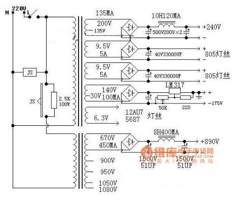
View full Circuit Diagram | Comments | Reading(2637)
PROPERTT_ALARM_CIRCUIT
Published:2009/7/12 22:43:00 Author:May

The circuit is designed to protect by means of a wire loop or mercury switch. TR1 and associated components form a switch that is biased off by the normally closed (N.C.) link. When the link is broken, TR1 conducts and triggers the thyristor (CSR1) into conduction. Consequently, the LED flasher centered around the 555 astable of IC1 causes D1 to blink. Additionally, IC2 is a monostable timer that triggers through R5/C2 and drives an audible warning device via TR2 for a period of approximately 2 min before resetting. When the audio alarm has timed out, the LED will continue to flash, and this can be cancelled by opening S1, which resets the thyristor. The quiescent current of the circuit is very low because of the high value of resistor R1. A mercury switch can be used in place of the wire link to act as an antitamper alarm, in which case care must be taken to avoid accidental contact with the mercury bead itself because it is highly toxic.
(View)
View full Circuit Diagram | Comments | Reading(977)
3_A_LOW_ROPOUT_REGULATOR_WITH_50_μA_QUIESCENT_CURRENT
Published:2009/7/16 20:51:00 Author:Jessie

The LT1529 is a 3-A, 0.6-V dropout regulator with 50-μA no-load quiescent current and only 16 μA IQ shutdown. This makes the LT1529 useful for battery-powered applications where both long battery life and high-load current surges are expected. At 1.5-A load current, dropout voltage is just 0.43 V. The LT1529 needs no external diodes to protect against reverse battery or reverse output current faults. This allows the LT1529 to be used for backup power situations in which the output is held high while the input is at ground or reversed. (View)
View full Circuit Diagram | Comments | Reading(792)
BOOTSTRAPPED_AMP_CURRENT_SOURCE
Published:2009/7/16 20:51:00 Author:Jessie
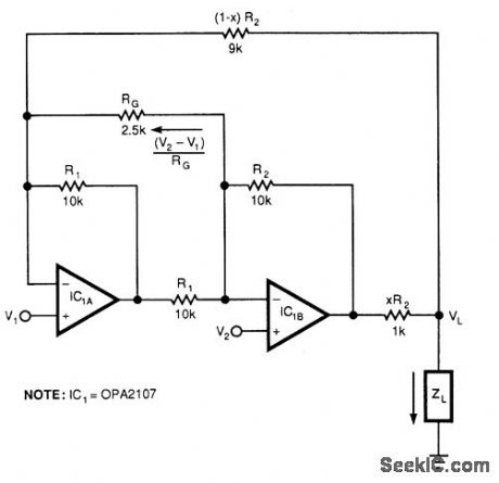
This circuit responds to the difference between V1 and V2. RG on sets gain. Resistors XR2 and (1 -X) R2 produce the bootstrap effect. These two resistors convert the circuit's output voltage to a current. IC1 and IC2 are Burr-Brown OPA2107 or equal. (View)
View full Circuit Diagram | Comments | Reading(742)
13_V_SUPPLY
Published:2009/7/16 20:51:00 Author:Jessie

This s a simple 1.3-V regulator to power the ZN414IC. (View)
View full Circuit Diagram | Comments | Reading(650)
1000_V_FOR_CRT
Published:2009/7/12 22:43:00 Author:May

Unique connection of two TV boostertransformers having 125-V secondaries gives high-voltage supply for small monitor scope. T1 is connected conventionally, with its 6.3 V winding going to heater of CRT, 6.3-V winding of T2, also connected to CRT, serves as primary for second transformer. Remaining windings of T2 and high-voltage secondary of T1 are connected in series aiding to give about 367 VAC fordoubling by D1-D2 and C1-C2. Since CRT drain is low, filter charges to very nearly peak voltage of 1027 VDC.-W. P. Tumer,Cheap Power Supply for a CRT, 73 Magazine, March 1974, p 53. (View)
View full Circuit Diagram | Comments | Reading(798)
MINI_POWER_SOURCE
Published:2009/7/16 20:50:00 Author:Jessie

The figure shows a unit capable of offering different voltages to operate low-voltage appliances from a 12-V battery. Regulators of the LM317 type are current-limiting, short- circuit-proof, and over-heat-proof, although they are still not indestructible. This circuit will provide up to 1.5 A. IC1 should be heatsinked, perhaps by bolting it with an insulating kit to a metal box. (View)
View full Circuit Diagram | Comments | Reading(716)
MICROSECONDS_TO_HOURS
Published:2009/7/12 22:42:00 Author:May
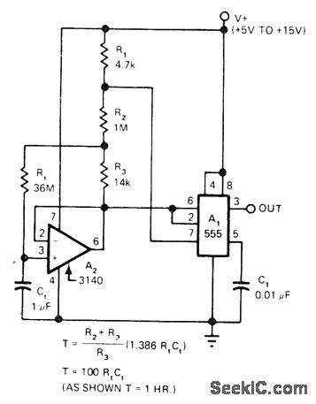
Timing range of 555 is increased 100 times by using 3140 FETinput opa mp in circuit that eff ectively multiplies values of timing components and buffers timing network, Pin 7 of 555 switches applied voltage of timing network between V+ and ground. Ratio selected for R2-R3 can be varied over wide range to change multiplying ratio, provided square-wave voitage across R3 is at least 50 mV. Output is essentially pure square wave. Supply voltage is notcritical.-W. G. Jung, Take a Fresh Look at New IC Timer Applications, EDN Magazine, March 20, 1977, p 127-135. (View)
View full Circuit Diagram | Comments | Reading(551)
FAST_DIFFERENTIAL_INPUT_CURRENT_SOURCE
Published:2009/7/16 20:50:00 Author:Jessie

An LT1022 op amp used in this configuration can provide a rapidly switched current source. Use the equations in the figure to select component values. (View)
View full Circuit Diagram | Comments | Reading(754)
1_YEAR_TIMER
Published:2009/7/12 22:41:00 Author:May

Cascaded operation of Exar XR-2242 long-range timers provides ultralong time delays, up to 1 year, Cascading of counter sections provides 32,640 clock cycles before output pin 3 of unit 2 changes state. Common pull-up resistor makes counter section of unit 2 trigger each time output of unit 1 makes positive-going transition. Cascading additional timer with unit 2 extends time delay to 1.065 x 10⁹RC. With RC values giving 0.1 s, time delay becomes 3.4 years.- Timer Data Book, Exar Integrated Systems, Sunnyvale, CA, 1978, p 19-22. (View)
View full Circuit Diagram | Comments | Reading(898)
SAFER_SECURITY_STSTEM
Published:2009/7/12 22:41:00 Author:May
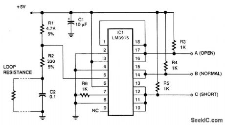
Many security systems use a closed loop of wires and switches, arranged so that whenever a door or window is opened, the loop will be broken and the alarm will sound. An obvious problem is that someone can tamper with the system, short out the loop, and later on come back and burglarize the premises without sounding the alarm. Hiding a known resistance in the loop is a very good idea. That way, the alarm can distinguish a short circuit from a correctly functioning closed loop. The figure shows a circuit that does the job. It is a somewhat unusual application for a National Semiconductor LM3915lC, normally used to drive LED bar-graph displays. That chip happens to contain the right combination of comparators and logic circuits to do what you need. Step 1 is to translate the loop resistance into a voltage. That is done by putting a voltage divider with resistors R1 and R2. Capacitor C2 protects the circuit against electromagnetic noise-important because burglar alarms use long wires, often running near heavy electrical equipment. Step 2 is to translate the voltage into a logic signal indicating whether it's in the correct range. Normally, the LM3915 would drive 10 LEDs, one for each of the small ranges of voltage. To obtain logic-level outputs, we have it driving 1-kΩ resistors instead of LEDs. Since we need to distinguish only three situations, we tie some of the outputs together. The LM3915 has open-collector outputs that can be paralleled in that way. Note that they use negative logic (0 V for yes, +5 V for no ), the opposite of ordinary logic circuits. You can use inverters, such as the 74HC04, to produce positive logic signals, if that's what you need. Finally, note that the circuit will actually work with any supply voltage from 3 to 25 V.
(View)
View full Circuit Diagram | Comments | Reading(783)
GASFET_POWER_SUPPLY
Published:2009/7/16 20:49:00 Author:Jessie

Suitable for use with the GASFET doubler In this text, and other similar applications, this supply delivers + 3 Vdc and 0 to -3 Vdc bias. (View)
View full Circuit Diagram | Comments | Reading(1023)
BMW7 Series EGS / EML 35pin Transmission Circuit (the 1st)
Published:2011/7/17 21:53:00 Author:Felicity | Keyword: BMW7 Series, EGS / EML 35pin, Transmission Circuit, (the 1st)

View full Circuit Diagram | Comments | Reading(951)
| Pages:743/2234 At 20741742743744745746747748749750751752753754755756757758759760Under 20 |
Circuit Categories
power supply circuit
Amplifier Circuit
Basic Circuit
LED and Light Circuit
Sensor Circuit
Signal Processing
Electrical Equipment Circuit
Control Circuit
Remote Control Circuit
A/D-D/A Converter Circuit
Audio Circuit
Measuring and Test Circuit
Communication Circuit
Computer-Related Circuit
555 Circuit
Automotive Circuit
Repairing Circuit