
Circuit Diagram
Index 748
Discharge type single trigger timing circuit formed by PUT
Published:2011/8/2 5:14:00 Author:Nancy | Keyword: Discharge type, single trigger , timing
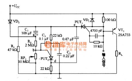
Figure 1 is the discharge type single trigger timing circuit formed by PUT. When there is no input signal, PUT1 cuts off, and so does the transistor VT1. At this time, C1 charges to the power supply voltage Ucc. If we add the input signal, PUT1 and VT1 conduct, current flows through the load RL. At the same time, the potential of point a is two times of the power supply voltage Ucc, C2 and C3 charge to the power supply voltage Ucc. From this time, C1 discharges through R2 and RP1, then the potential of point a drops slowly. After reaching the set time, if the potential of point b is lower than that of point c, then PUT conducts.
(View)
View full Circuit Diagram | Comments | Reading(529)
PHOTOMULTIPLIER_TUBE_SUPPLY
Published:2009/7/16 21:49:00 Author:Jessie

This circuit is quite efficient, drawing virtually no current when the load is a photomultiplier (PM) used as a scintillation detector. Be sure that the voltage-divider resistors on the PM tube are very high to conserve power-the higher the better. If the high-voltage circuit uses a diode voltage-multiplier chain, then connect the chain to the transformer, just as the three-diode doubler is connected. Lower the regulated voltage by removing one of the neons or by selecting an appropriate zener. If a higher voltage is needed, simply extend the diode multiplier. (View)
View full Circuit Diagram | Comments | Reading(2264)
ANALOG_CHARACTER_GENERATOR
Published:2009/7/16 21:49:00 Author:Jessie
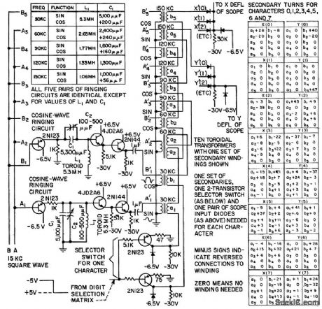
Displays numeric characters 1 through 7 on cathode-ray tube by deflecting spot to trace out each character continuously. X and Y defection voltages are obtained by combining sine and cosine terms of first five harmonics of 30-kc fundamental. Transistorized gated oscillators, flip-flop serial counters, and emitter -followers feed 10 toroidal transformers having one sot of secondary windings for each character.-K. E. Perry and E. J. Aha, Generating Characters for Cathode-Ray Readout, Electronics, 31:1, p 72-75. (View)
View full Circuit Diagram | Comments | Reading(802)
HELIUM_NEON_LASER_POWER_SUPPLY_WITH_HV_PULSE_IGNITION
Published:2009/7/16 21:48:00 Author:Jessie

The helium-neon laser requires two voltages: a voltage in the range of 10 kV that starts the laser and then turns off once the discharge begins, and a lower-voltage power supply to sustain the dis-charge. The circuit diagram illustrates one method of generating the laser ignition voltage. A fraction of the main supply voltage is used to charge up a capacitor. When triggered, it is discharged through a high-voltage ignition transformer in series with the main power supply output. When the supply is first turned on, a delay circuit allows the main supply to stabilize at full voltage and charge up the capacitor. A nonlatching relay operates to discharge the capacitor into the ignition coil on a one-shot basis after the timing delay. The HV diode in series with the ignition coil and the capacitor across the supply rectifies the damped oscillatory waveform out of the ignition coil, producing a single positive pulse across the laser tube to ionize the gas in the laser. Once the laser is ignited by the HV pulse, the main power supply maintains the discharge. (View)
View full Circuit Diagram | Comments | Reading(3338)
FINE_POSITIONING_CHARACTER
Published:2009/7/16 21:47:00 Author:Jessie

GENERATOR SWTICH-Pairs of deflection Switches operating push-pull into defection yoke act with 16-point coarse positioning system to give 4,096 positions, generated in binary fashion.-K.E Perry and E.J. Aho, Radar-Computer Display fracas Alphanumeric Characle,Electronics,34:26,p 75-79. (View)
View full Circuit Diagram | Comments | Reading(787)
Overcurrent protection circuit diagram
Published:2011/7/20 5:06:00 Author:nelly | Keyword: Overcurrent, protection

View full Circuit Diagram | Comments | Reading(563)
REGULATOR_FOR_700_V_LOW_CURRENT_SUPPLY
Published:2009/7/16 21:45:00 Author:Jessie

If you need a regulated output, change the voltage doubler to a tripler, and use neon lamps as a regulator. The number of lamps you will need will depend on the characteristics of the lamps used, and will have to be found by experimentation. Each lamp has approximately a 55- to 70-V the break-down voltage. The lamps should be shielded from light (or painted black) because light can influence the breakdown voltage. (View)
View full Circuit Diagram | Comments | Reading(634)
GEIGER_COUNTER_700_V_LOW_CURRENT_SUPPLY
Published:2009/7/16 21:45:00 Author:Jessie

This 700-V, 0.25-mA power supply converts a +9-Vdc input to 10-kHz ac, then uses the setup transformer and the voltage-doubler circuit to produce the required output. (View)
View full Circuit Diagram | Comments | Reading(1420)
Long time delay circuit formed by the power MOSFET
Published:2011/7/26 10:06:00 Author:Nancy | Keyword: Long time delay, power MOSFET

Figure 1 is a long time delay circuit formed by the power MOSFET. The grid input impedance of the power MOSFET is very high, so it is easy to choose the resistor and capacitor with large grid time constant. When the gate opens, the gate control switch S1 conducts, the base of VT1 is low level and in the conduction state, so the grid of the power MOSFET (VT2) is high level and conducts, the indoor light H is lit up. When the gate is closed, the gate control switch S1 disconnects, the base of VT1 is high level and cut off. However, the time constant formed by the R1 and C1 make VT2 conduct for lOs, which keeping the grid voltage of VT2 higher than threshold voltage. With the discharge of C1, the grid voltage of VT2 reduces and cuts off, the indoor light H burns out. (View)
View full Circuit Diagram | Comments | Reading(1879)
Regulated power supply circuit diagram with adjustable transistor output voltage
Published:2011/7/20 5:10:00 Author:nelly | Keyword: Regulated power supply, transistor, output voltage

View full Circuit Diagram | Comments | Reading(1872)
BASIC_CHARGE_PUMP_CIRCUIT
Published:2009/7/16 21:44:00 Author:Jessie

A basic charge pump provides voltage doubling or inversion. It can be implemented with on-chip switches (a) or discrete diodes (b). (View)
View full Circuit Diagram | Comments | Reading(889)
4_WAY_LOGIC_PROBE
Published:2009/7/16 21:44:00 Author:Jessie

This logic probe has four channels and uses two IF quad comparators to drive four bicolor LEDs. S1 and S1B program the comparator trip levels for TTL and CMOS. R6 through R13 bias the probe inputs to prevent the probe from indicating a HIGH for an open circuit. An open circuit will produce an OFF indication on the LED. The LEDs will indicate one color for high, the other color for low, and intermediate colors for pulsing (assuming a duty cycle between 30 and 70%). The color that corresponds to HIGH or Low depends on how you connect the LEDs. (View)
View full Circuit Diagram | Comments | Reading(1506)
DYNAMIC_MICROPHONE_PREAMP
Published:2009/7/16 21:42:00 Author:Jessie

This circuit uses a TL082 op amp to boost the output of a dynamic mike to a level sufficient for a radio transceiver, audio amplifier, or PA system. (View)
View full Circuit Diagram | Comments | Reading(8379)
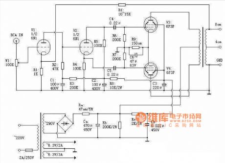
6P3P Push-pull Tube Amp Circuit
Published:2011/7/17 23:43:00 Author:Felicity | Keyword: 6P3P, Push-pull, Tube Amp Circuit
View full Circuit Diagram | Comments | Reading(4713)
UNIVERSAL_TEST_PROBE
Published:2009/7/16 21:42:00 Author:Jessie

The compact test prbbe provides rapid measurement of voltage levels at digital gates, fuses, diodes, batteries, and others. It does not provide absolute values, but rather it provides a good indication of correct operation or otherwise.
Measurements are carried out with pins A and B. If the potential difference between A (the reference pin) and B is 1.9 to 2.0 V, D2 will light. If the voltage at B is ≤ 1.4 V higher than that at A, D3 will light. Finally, if the potential at B is a 11 V, with respect to that at A, D1 will light.
Transistor T5 is used as a zener diode. The probe allows the measurement of alternating voltage. The maximum input voltage is highly dependent on the dissipation allowed in R1. For example, when this resis-tor is a 0.5-W type, the input voltage can be as high as 200 Vrms.
The current drawn by the circuit depends on the number of lighting LEDs: it is not more than 10 mA at a supply voltage of 3 V. In quiescent operation, the current is so low (about 5μA) that an on/off switch is not necessary. (View)
View full Circuit Diagram | Comments | Reading(716)
ELECTRET_MIKE_CIRCUIT
Published:2009/7/16 21:41:00 Author:Jessie

This circuit shows how to power an electret microphone. The 5-kΩ potentiometer acts as a gain control. (View)
View full Circuit Diagram | Comments | Reading(889)
HELIUM_NEON_LASER_SUPPLY_WITH_HV_MULTIPLIER_IGNITION
Published:2009/7/16 21:40:00 Author:Jessie

This figure illustrates a way in which a momentary 10-kV voltage pulse can be generated to initiate the plasma discharge across the laser tube. A Diode voltage-multiplier circuit is connected in series with the main supply and obtains its input power across one of the voltage-multiplier diodes in the main supply. The voltage across this diode is typically 1.8 kV p-p With a ten-section multiplier, the output voltage is approximately 9 kV in series with a 1.8-kV sustaining supply. The capacitors value of the capacitors in the multiplier chain is much smatter than that of the capacitors for the main supply. When the power supply is first turned on, the capacitors in the voltage multiplier charge up to the ignition voltage. As the plasma forms, the laser tube draws more current and the multiplier capacitors cannot maintain their charge. As a result, the voltage immediately drops to that of the main sustaining supply, with all the diodes in the multiplier chain forward-biased. In this manner, an HV pulse is generated to ionize the gases. (View)
View full Circuit Diagram | Comments | Reading(4508)
BLOOD_OXYGEN_MEASUREMENT
Published:2009/7/16 21:39:00 Author:Jessie

An oximeter measures the amount of oxygen in your blood by shining light through some part of your body-traditionally the earlobe, nowadays often the finger-and comparing the transmission of two different wavelengths, 800 nm (in the near infrared) and 640 nrn (bright red). If they're about the same, your oxygen is very low; if your blood is well oxygenated, the 640-nm transrnission will be much higher. The light sources are LEDs, and the detector is a silicon photodiode or phototransistor. (View)
View full Circuit Diagram | Comments | Reading(1397)
LOGIC_TESTER
Published:2009/7/16 21:39:00 Author:Jessie

The input consists of two comparators that operate with different reference voltages supplied by separate potential dividers. Divider R3/R4/R5 provides a voltage of about 40% of the supply voltage, UCC, to pin 6 of IC1B and one of about 16% of UCC to pin 3 of UC1A. When UCC = 5 V, these voltages are exactly the thresholds (0.8 and 2.0 V) of the TTL comparators.
Similarly, divider R6/R7/R8 provides voltages of 23% of UCC and 73% of UCC to pin 3 of IC1A and pin 6 of IC1B respectively; these levels correspond to the standard threshold for CMOS comparators.
The voltage to be measured Ua, is applied to pin 5 of IC1B and pin 2 of IC1A and compared with the respective reference. The output of comparator IC1B goes high when Ua, exceeds the reference, whereas the output of IC1A goes high when Ua lies below the voltage at pin 3.
The comparators are followed by driver stages, T1 and T2, for the LED display (D1 for high and D2 for low ) and also NOR gate IC2A that switches on T3 when the output of both comparators is low, that is, when it is undefined. This state is indicated by D3.
The remaining three gates in IC2 form a monostable. During quiescent operation, UCC is present at the input of inverter IC2C. The output of the inverter is then low, T4 is off and D4 is out. Pin 4 of IC2B is also high, but this state changes when a pulse arrives at pin 5. The output of IC2B then goes low, C2 discharges, the inverter toggles, T4 is switched on, and D4 lights. This state is unstable, however, because C2 recharges via R13, Although the pulse at pin 5 might be very short, the time constant R13/C2 lengthens it to about 100 ms.
The supply voltage can lie between 5 and 15 V. At 5 V, the circuit draws a current of about 15 mA. The input impedance of the tester is of the order of 330 kΩ. (View)
View full Circuit Diagram | Comments | Reading(937)
HEART_SOUND_SIMULATOR
Published:2009/7/16 21:38:00 Author:Jessie

This oscillator circuit imitates the sound of a heartbeat. Use a 4-in or larger speaker to get good bass response. (View)
View full Circuit Diagram | Comments | Reading(1112)
| Pages:748/2234 At 20741742743744745746747748749750751752753754755756757758759760Under 20 |
Circuit Categories
power supply circuit
Amplifier Circuit
Basic Circuit
LED and Light Circuit
Sensor Circuit
Signal Processing
Electrical Equipment Circuit
Control Circuit
Remote Control Circuit
A/D-D/A Converter Circuit
Audio Circuit
Measuring and Test Circuit
Communication Circuit
Computer-Related Circuit
555 Circuit
Automotive Circuit
Repairing Circuit