
Circuit Diagram
Index 752
MISSING_PULSE_DETECTOR
Published:2009/7/16 23:34:00 Author:Jessie

Detects presence or absence of pulse train and indicates whether level remains positive or negative after pulsing stops.-R. W. Allington, Pulse Absence Detector, FEE, 11:5, p 90-91. (View)
View full Circuit Diagram | Comments | Reading(0)
PULSE_SEQUENCE_DETECTOR
Published:2009/7/16 23:32:00 Author:Jessie

Resistor divider between Q1 and Q2 supplies current to silicon controlled switch Q1 after it is trig-gored by pulse at input A. Divider also pre vents input B from triggering Q2 until after Q1 conducts.- Transistor Manual, Seventh Edition, General Electric Co., 1964, p 428. (View)
View full Circuit Diagram | Comments | Reading(1264)
EXTENDED_68HC11_RESET_TIMEOUT
Published:2009/7/16 23:32:00 Author:Jessie
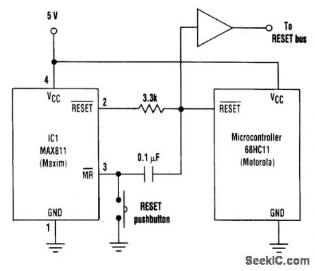
Some microcontrollers (such as the Motorola 68HC11) are implemented with a bidirectional RESET pin that can create a contention problem with the RESET output of certain supervisory ICs. If the supervisor RESET is high, for example, and the microcontroller tries to pull it low, the result might be an intermediate logic level that fails to reset the microcontroller. In addition, some devices on the RESET bus might require a RESET pulse of longer duration than the microcontroller pro-vides. IC1 in the circuit shown eliminates this concern by producing a RESET output with a mini-mum duration of 140 ms. Its RESET output becomes asserted either when the microcontroller initiates a reset, when the MR pushbutton is depressed, or when VCC dips below a threshold internal to IC1. When the reset line is pulled low by IC1 or the microcontroller, MR is pulled low and then re-turns high (initiating a timeout period of 200 ms typical) as the capacitor is charged via the internal MR pull-up resistor. 1C1's RESET deasserts following the timeout, allowing the capacitor to discharge through the internal pull-up resistor and ESD-protection diode. (View)
View full Circuit Diagram | Comments | Reading(872)
ANTICOINCIDENCE_DETECTOR
Published:2009/7/16 23:31:00 Author:Jessie

Gives indication whenever two input pulses are not coincident. Limit on smallest degree of anticoincidence that is detectable is determined by turn-on time of SCR’s, and is about 0.3 microsec for 2N1595 scr used, when C1 is omitted. Upper limit is set by C1, and can be several tenths of a second when C1 is 200 mfd. Circuit is reset by interrupting supply. Diodes are 1N691, and lamp is 1819.-J. T. Gatshal, Anti-Coincidence Detector, EEE, 10:9, p 28-29. (View)
View full Circuit Diagram | Comments | Reading(670)
GUARD_DRIVE
Published:2009/7/16 23:30:00 Author:Jessie

A guard drive can improve common-mode rejection and ac gain when an IA includes an RC circuit made up of the sensor source resistance and the capacitance associated with a coax cable (a). The guard drive prevents a voltage from developing across the capacitance, thus eliminating it from the RC filter's equivalent circuit (b). (View)
View full Circuit Diagram | Comments | Reading(607)
BURGLAR_ALARM
Published:2009/7/12 22:28:00 Author:May

This burglar alarm uses either normally closed (S5 to S8) or normally open (S9 to S11) switches or a combination thereof. Activation sets latches IC1-b and IC1-c. S1 is used to disarm the circuit. IC1-d and related components drive switch Q1, which triggers timer IC2. IC2 generates a pulse, determined by R3 and C5, that energizes alarm relay RY1. S2 allows for a continuous alarm and S12 is a panic switch to sound the alarm immediately. Either a built-in buzzer (BZ1) or an external siren can be used as an annunciator. (View)
View full Circuit Diagram | Comments | Reading(0)
30_s_NONRETRIGGERABLE
Published:2009/7/12 22:28:00 Author:May
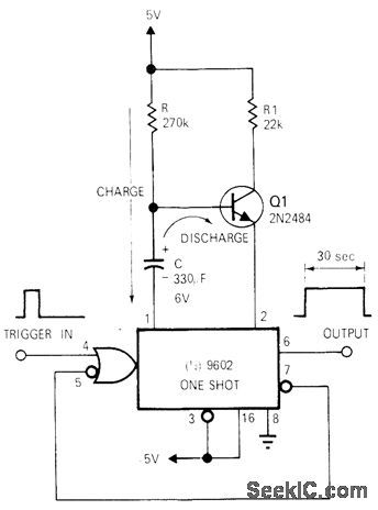
With values shown, rnono IC gives delay period of 30 s after triggering by input pulse and ignores other input pulses during timing period. Delaytimein seconds is RC/3, where R is in ohms and C in farads. Delay can be reduced to as little as 10ms by reducing R to 30 kilohms and C to 1 μF. Maximumdelay is about 1 min, with 560 kilohms for R.-F. R. Shirley, Thirty-Second Timer Uses IC One-Shot, EDNIEEE Magazine, Jan. 1, 1972, p 73-74. (View)
View full Circuit Diagram | Comments | Reading(597)
LOW_VOLTAGE_POWER_CONTROLLER
Published:2009/7/12 22:27:00 Author:May

The circuit has a duty-cycle generator that produces an output varying from fully off to fully on and pulses of any duty cycle in between the two extremes. The circuit can be fed from any dc supply source of between 10 and 15 V. U1-a and U2-a combine to form a voltage-to-pulse-width converter. The first half of the dual oscillator/timer is configured as an astable oscillator, generating a continuously oscillating ramp voltage, Op amp U2-a compares the voltage at its noninverting input to the voltage at its inverting input. The op amp will give a low output if R1's wiper voltage is higher than the instantaneous voltage present at pins 2 and 6 of U1-a. The output of U2-a at pin 2 will have an on/off ratio that is proportional to the voltage at RI's wiper. Because the output of U2-a does not have enough power-handling capacity to drive the MOSFET its output is fed to U1-b, which is used to bufferthe signal. The low-impedance, pulsed output of U1-b at pin 9 is fed to the gate of MOSFET Q1, driving it hard on or off. Diode D1 is used to suppress the reverse-voltage spikes generated by inductive loads during turn-off. If the circuit will not be used to drive inductive loads (motors), D1 can be eliminated. Note: This controller can be used only with incandescent lamps and permanent-magnet dc motors. (View)
View full Circuit Diagram | Comments | Reading(0)
_5_7AND__10V
Published:2009/7/16 23:30:00 Author:Jessie


Developed to meet power requirements of RTTY message generator having ITL and Numitrons requiring +5 V and MOS RAM requiring negative voltages. Diagram shows how to add 12-V storage batteries to prevent loss of programming if AC power fails momentarily.-B, Kelley, Random Access Memory RTTY Message Generator, Ham Radio, Jan.1975, p 8-15. (View)
View full Circuit Diagram | Comments | Reading(569)
LINEAR_PULSE_WIDTH_CONTROL
Published:2009/7/16 23:28:00 Author:Jessie

Blanking pulse generator provides blanking signal starting with input pulse and remaining on for some nominal portion of pulse, regardless of dropouts due to noise in triggering pulse.-blanking Pulse Generator with Linear Pulse Width Control, Electronic Circuit Design Handbook, Mactier Pub. Corp., N.Y., 1965, p 78. (View)
View full Circuit Diagram | Comments | Reading(563)
1_s_H_16_H_PRECISION
Published:2009/7/12 22:26:00 Author:May
Accuracy is comparable to that of 60-Hz power-line frequency. After Fladio Shack 276-561 6-V zener divides powerline frequency by 2, 7490 decade counter provides division by 10 to give 3 Hz. 555 timer connected as mono MVBR is then adjusted with R4 to divide by 3. LED then flashes at precise 1-s intervals, staying on about 100 ms, T1 is 6.3-V filamenttransf ormer.-F. M. Mints, Integrated Circuit Projects, Vol. 5, Radio Shack, Fort Worth, TX, 1977, 2nd Ed., p 21-29. (View)
View full Circuit Diagram | Comments | Reading(1156)
±6_V_AND_±15_V
Published:2009/7/16 23:28:00 Author:Jessie

Developed for use with wide-range function generator requiring these voltages for transistors and ICs. Voltage-setting 15K and 37.5K resistors are adjusted to give de-sired output voltages.-H. Olson, The Function Generator, CQ, July 1975, p 26-28 and 71-72. (View)
View full Circuit Diagram | Comments | Reading(0)
HUMAN_BODY_MODEL
Published:2009/7/16 23:26:00 Author:Jessie

The human-body model (HBM) is approximated with a series capacitor and resistance (a); the machine model (MM) is simply a capacitor (b). The model is charged to the required test voltage (V+) and switched into the device. If the input capacitance of the device (CISS) charges to higher-than-rupture voltage, the device will be destroyed. (View)
View full Circuit Diagram | Comments | Reading(637)
PULSE_PHASE_SPLITTER_1
Published:2009/7/16 23:26:00 Author:Jessie

Provides bipolar pulses 180°out of phase, with perfect coincidence of negative-going trailing edges, same reference level, and drive capability for saturated inverters. Used for switching sample-hold gates requiring opposite-going pulses with trailing-edge coincidence.-G. Wolff, Simple Pulse Phase-Splitter, EEE, 14:2, p 70-72. (View)
View full Circuit Diagram | Comments | Reading(816)
GENERIC_TRIAC_SWITCH_INTERFACE_FOR_INDUCTIVE_LOAD
Published:2009/7/16 23:26:00 Author:Jessie

A TTL level input turns on the MOC3010 optocoupler and triggers the triac, applying 120 Vac to the load. (View)
View full Circuit Diagram | Comments | Reading(3690)
±15_V_TRACKING
Published:2009/7/16 23:25:00 Author:Jessie

Uses Motorola dual-polarity regulator to provide balanced positive and negative voltages, with series-pass transistor handling major part of output current. Developed for use with audio signal generator.- H. Olson, Integrated-Circuit Audio Oscillator, Ham Radio, Feb. 1973, p 50-54. (View)
View full Circuit Diagram | Comments | Reading(0)
PHOTOVOLTAIC_ISOLATOR_WITH_FAST_RESET_1
Published:2009/7/16 23:23:00 Author:Jessie

The combination of a weak photovoltaic isolator pull-up and a strong programmable junction transistor pull-down leads to a very simple half-bridge FET or IGBT driver, which virtually guarantees that the devices won't crowbar the power supply. The device turning off will do so rapidly, but the device turning on will do so very slowly. A dead time is inherent in the circuit dynamics, so no additional circuitry is required to prevent a crowbar or shoot-through effect. (View)
View full Circuit Diagram | Comments | Reading(3226)
MEASURING_PULSE_LENGTH
Published:2009/7/16 23:23:00 Author:Jessie
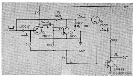
Circuit delivers output pulse only when triggered by input pulse above preset width. Can be used for checking lengths of objects moving past photocell.-K. R. Whittington and G. Robson, Versatile Discriminator Measures Pulse Length, Electronics, 35:31, p 48. (View)
View full Circuit Diagram | Comments | Reading(860)
Zhonghua Car Air Conditioning System Circuit(the 2nd)
Published:2011/7/18 5:05:00 Author:Felicity | Keyword: Zhonghua Car, Air Conditioning System, Circuit

View full Circuit Diagram | Comments | Reading(570)
IMPROVED_ULTRA_LONG_MONO
Published:2009/7/16 23:21:00 Author:Jessie

Eliminayion of reset transistor and coupling diode makes circuit insensitive to supply bus transients, cuts standby current to essentially zero, and improves efficiency under heavy loading. Will handle loads above 150 ma.-J. C. Schaeffert and N. F. Goldman, Improved Ultra-Long Monosable Multivibrator, EEE, 12:12, p 57-58. (View)
View full Circuit Diagram | Comments | Reading(519)
| Pages:752/2234 At 20741742743744745746747748749750751752753754755756757758759760Under 20 |
Circuit Categories
power supply circuit
Amplifier Circuit
Basic Circuit
LED and Light Circuit
Sensor Circuit
Signal Processing
Electrical Equipment Circuit
Control Circuit
Remote Control Circuit
A/D-D/A Converter Circuit
Audio Circuit
Measuring and Test Circuit
Communication Circuit
Computer-Related Circuit
555 Circuit
Automotive Circuit
Repairing Circuit