
Circuit Diagram
Index 759
BAUD_RATE_GENERATOR
Published:2009/7/12 22:07:00 Author:May
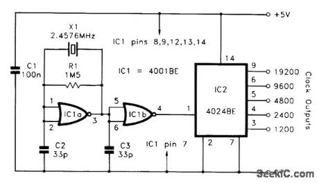
Gate IC1a is used in a conventional crystal oscillator circuit and IC1b acts as a buffer stage. IC2 is a CMOS 4024BE seven-stage binary counter and its clock input is fed with the 2.4576-MHz signal from IC1b. The first two stages of IC2 are not used, but the other five outputs provide baud rates from 1200 to 19,200 baud. Of course, the clock frequency is 16 times the baud rate and output frequencies from IC2 range from 19.2 to 307.2 kHz. (View)
View full Circuit Diagram | Comments | Reading(2047)
_13_V_AT_1_A
Published:2009/7/17 1:31:00 Author:Jessie

Regulated output voltage can be varied upward about 0.6 V per diode by placing silicon diodes between pin 3 and ground. Two diodes boost output of regulator from 11.9 V to about 13 V. Insulate regulator from heatsink with mica washers. CR1 and CR2 are 50-PIV 3-A diodes. Motorola equivalent of regulator is MC7812.-A. M. Clarke, Simple, Super regulated, 12 Volt Supply, CQ, April 1974, p 61-62. (View)
View full Circuit Diagram | Comments | Reading(784)
FOUR_QUADRANT_ANALOG_MULTIPLIER
Published:2009/7/17 1:31:00 Author:Jessie
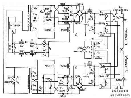
Uses two square-law multiplier circuits con taining only magnetic cores, silicon diodes, and resistors, to provide first square term of algebraic sum of currents I1 and I2, and second square term of difference of these cur rents.-J. Markus, Handbook of Electronic Control Circuits, McGraw-Hill, N.Y. 1959, p 104. (View)
View full Circuit Diagram | Comments | Reading(584)
AMPLIFIER_FOR_10_NSEC_PULSES
Published:2009/7/12 22:06:00 Author:May
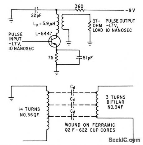
Requires accurately wound pulse transformer in which secondary is close-wound over end of primary that is a-c ground, with accurate control of unsymmetrical distributed capacitance,to serve as building block of 50-megapulse computer. Commercial equivalent of L-5447 is 2N769 or 2N976.-K. H. Konkle and J. E.Laynor, Key to Faster Computers: Ten-Nano-second Amplifier, Electronics, 35:50, p39-41. (View)
View full Circuit Diagram | Comments | Reading(634)
DIFFERENTIAL_MAGNETIC_INVERTER
Published:2009/7/17 1:30:00 Author:Jessie
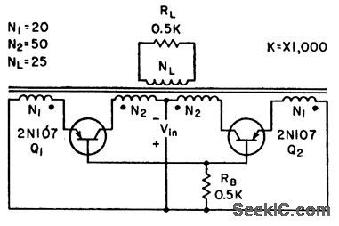
Oscillates reliably without use of current bias. Excessive drive will not cause transistor overheating. Differential action of collector and emitter windings greatly improves performance as compared to conventional nondif-ferential inverter and eliminates need for clipping diodes.-J. Markus, Handbook of Electronic Control Circuits, McGraw-Hill, N.Y., 1959, p 103. (View)
View full Circuit Diagram | Comments | Reading(553)
COMPLEMENTARY_FADER_
Published:2009/7/12 22:03:00 Author:May


Control unit for stage lighting fades out one lamp while simultaneously increasing light output of another with accurate tracking. Gate of silicon controlled rectifier SCR1 is driven by standard external phase control circuit. Interlock network connected to output of SCR1 provides complementary signal for trigger of SCR2. If lamps larger than 150 W are required, use largervalue for C1.-M. E. Anglin, Complementary Lighting Control Uses Few Parts, Electronics, Dec. 12, 1974, p 111; reprinted in Circuits for Electronics Engineers, Electronics, 1977, p 78.
(View)
View full Circuit Diagram | Comments | Reading(541)
SEVEN_SEGMENT_LOGIC_PROBE
Published:2009/7/17 1:29:00 Author:Jessie

This circuit is capable of indicating the HI or LO status of a digital circuit. The circuit in the figure will display the letter H for HI or +5 V and L for LO or 0 V. The 2N2222 NPN transistor serves as a driver for turning on the appropriate segments of the display, thereby producing the letter H. This condition will occur with a + 5-V signal applied to the base of the transistor. If a 0-V signal is detected at the base of the transistor, the letter L will be displayed, indicating that the transistor driver is turned off. (View)
View full Circuit Diagram | Comments | Reading(881)
CHOKE_CONTROLLED_DIFFERENTIATOR
Published:2009/7/12 22:00:00 Author:May

Uses inductance to control on time of transistor.Can also be used as staightforward pulse inverter,Input pulse is wider than output pulse.-W. M. Carey, Using Inducfive Control in Computer Circuits, Electronics, 32:38, p31-33. (View)
View full Circuit Diagram | Comments | Reading(493)
CONSTANT_OFF_TIME_REGULATOR_WITH_FREQUENCY_COMPENSATION
Published:2009/7/17 1:39:00 Author:Jessie

Constant off-time switching regulators offer several advantages over constant-frequency designs The only potential problem is that the switching frequency Increases with nsmg input voltage In designs that have large ratios of the high line to low-line supply voltage,this frequency shift can get quite large As a result,the switching losses can become excesslve at high input voltages To offset this problem,the simple circuit shown detects the high input voltage condition and lowers the switching frequency to keep switching losses under control The frequency-shift circuit consists of D3,R8,Q1,and C12 When Vin exceeds the zener voltage plus the FET threshold,Q1 turns on and adds an extra timing capacitor(C12) in parallel with the timing capacitor (C10) This increases the off-time,lowering the frequency. (View)
View full Circuit Diagram | Comments | Reading(1486)
DUAL_LAMP_DRIVER
Published:2009/7/12 21:59:00 Author:May

National DS75451 dual peripheral AND driver using positive logic provides up to 300 mA per section for driving incandescent lamps. Optional keep-alive resistors R maintain OFF-state lamp current at about 10% of rated value to reduce surge current.Lamp voltage depends on lamps used. Relays shown, with diodes across solenoids, can be used in place of lamps if desired.- Interface Databook, National Semiconductor, Santa Clara, CA, 1978, p 3-20-3-30. (View)
View full Circuit Diagram | Comments | Reading(679)
SCOPE_PROBE_CIRCUITS
Published:2009/7/17 1:40:00 Author:Jessie

Assuming a 1-MΩ Scope input impedance and input capacitance Cin, Ccompensation=(Rprobe/1 MΩ) Cprobe or Cprobe /Cinput = Rinput/Rprobe. (View)
View full Circuit Diagram | Comments | Reading(662)
LONG_TURNOFF_DELAY
Published:2009/7/12 21:59:00 Author:May

Combination of timer, optoisolator, and bridge-triggered triac keeps AC motor or other device energized for up to 1 h after control switch is depressed momentarily. Closing of switch drops voltage at pin 2 of timer below 1/3 VCC, making timer output go high and thus tum LED on. At same time, capacitor at pin 7 begins charging. Output re-mains high until oapacitor reaches 2/3 VCC, when outputis reset to low state and motor thereby turned off.-T Mazur,Solid-State Relays Offer New to Soutions to Many Old Problems, EDN Magazine, Nov 20,1973,p 26-32. (View)
View full Circuit Diagram | Comments | Reading(1377)
SEQUENTIAL_TIMER
Published:2009/7/12 21:57:00 Author:May
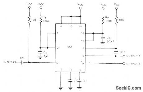
Output offirst ham of 556 dual timeris fed to input of second half through 0.001-μF coupling capacitor to give total delayequal to sum of individual timer delays,First half of timer is started by connecting pln 6 momentarily to ground After interval determinedby 1.1R1C1,second timer starts its delay determinod by 1.1R2C2- Signetics Analog Data Manual, Signetits、Sunnyvale,CA,1977,p724. (View)
View full Circuit Diagram | Comments | Reading(0)
PULSE_SHAPER_FOR_600_KC_CLOCK
Published:2009/7/12 21:57:00 Author:May


Oscillator input through Q1 switches Q2 on,and same input fhrough Q3 switche Q2 of afer fixed delay, to produce desired rectangular clock pulse.-S.Schoen,Transistors Provide Computer Clock Signals, Electronics, 32:9, p70-72. (View)
View full Circuit Diagram | Comments | Reading(547)
STABLE_FOUR_TRANSISTOR_TIMER
Published:2009/7/12 21:56:00 Author:May
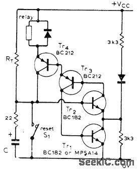
Circuit has good immunity to impulse noise because normal state of all transistors is on. This eliminates spurious timing cycles that sometimes occur in IC timers. At switch-on, C begins charging until its voltage makes Tr2 start conducting; this in turn makes other three transistors switch on. Regeneration action then discharges C to about 0.6 V. Timer is started either by applying VCC or opening S1. Timing period depends on value of VCC.-J. L. Linsley Hood, One-Shot Timer Circuit, Wireless World, Nov. 1975, p 520. (View)
View full Circuit Diagram | Comments | Reading(829)
PHASE_SHIFTER
Published:2009/7/12 21:55:00 Author:May

This circuit adds 120 degrees of phase shift to a 50- or 60-Hz input, regardless of the frequency and amplitude fluctuations of that input. The circuit configures a 2N4093 JFET as a voltage-controlled resistor whose value is proportional to the phase difference between the input and the output. The values of C1 R1 and rDS determine the amount of phase shift (120°this case.)A 555 timer implements a phase detector whose two inputs are related to the input and output. The input and output, respectively, drive IC1B and IC1C, which operate as zero-crossing detectors. D1 and D2 limit the positive-going pulse's at the 555 inputs. Thus, the falling edges of IC1B and IC1C's outputs control the 555 timer. The timer's output signal stays low for a time that is proportional to the phase shift between the circuit's input and output.The average value of the timer's output and an offsetting voltage drive IC1D. R2 and C2 filter IC1D's output. The resultant signal controls the JFET. The potentiometer sets the control at a value for which the phase shift between input and output is equal to 120 degrees when the input signal frequency is 50 or 60 Hz. Any differences between the input and output changes the 555 output's average value, thus ultimately modifying the control voltage and the JFET's resistance.To calibrate the circuit, apply a 50-Hz sine wave with an amplitude of less than 1 Vpp to the input and adjust the potentiometer until the phase shift reads 120°on a digital phase meter. For input frequency variations between 40 and 60 Hz, the phase shift changed by a maximum of ±0.17% (equivalent to an offset of only 0.02°/Hz). The average value at IC1D's noninverting input is 3.864 V. (View)
View full Circuit Diagram | Comments | Reading(4623)
SEQUENCED_TIMERS
Published:2009/7/12 21:54:00 Author:May
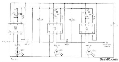
Cascading of three 555 timels, each driving LED, gives sequenced flashes with individually adjustable durations. Times of timers are determined by values used for C1, C3, and C5. R1, R3, and R5 values also affect time delays; use pots if 1 μF is used forall three capacitors.-F. M. Mints, Integrated Circult Projects, Vol. 5, Radio Shack, Fort Worth, TX, 1977, 2nd Ed., p 64-75. (View)
View full Circuit Diagram | Comments | Reading(889)
MARKER_PULSE_GENERATOR
Published:2009/7/12 21:53:00 Author:May

Uses blocking oscillator to generate digit pulses of word being stored in magnetic-spoke disk memory, as well as for generation of index marker pulses.-T.C. Chen and O. B. Stram, Digital Memory System Keeps Circuits Simple,Electronics, 32:11, p130-133. (View)
View full Circuit Diagram | Comments | Reading(1024)
SCSI_SWITCH
Published:2009/7/12 21:51:00 Author:May

The SCSI switch consists of an eight-position DIP switch, about 24 inches of ribbon cable, and eight female header blocks. A schematic of the switch is shown. The header blocks plug onto the ID pins of the SCSI hard disks. Through the DIP switch, those IDs can be reassigned at will. In any given configuration, whichever physical drive has the lowest SCSI ID becomes the boot drive. The others are allocated in order by SCSI ID. (View)
View full Circuit Diagram | Comments | Reading(684)
NONDIFFERENTIAL_MAGNETIC_INVERTER
Published:2009/7/17 1:45:00 Author:Jessie

Is analogous to free-running capacitor-coupled mvbr. Frequency and output amplitude are both directly proportional to input voltage. Chief drawback is need to increase input voltage to get higher frequency, which in turn increases all winding voltages.-J. Markus, Handbook of Electronic Control Circuits, McGraw-Hill, N.Y., 1959, p 102. (View)
View full Circuit Diagram | Comments | Reading(625)
| Pages:759/2234 At 20741742743744745746747748749750751752753754755756757758759760Under 20 |
Circuit Categories
power supply circuit
Amplifier Circuit
Basic Circuit
LED and Light Circuit
Sensor Circuit
Signal Processing
Electrical Equipment Circuit
Control Circuit
Remote Control Circuit
A/D-D/A Converter Circuit
Audio Circuit
Measuring and Test Circuit
Communication Circuit
Computer-Related Circuit
555 Circuit
Automotive Circuit
Repairing Circuit