
Circuit Diagram
Index 746
5_10_15_20_V_SWITCH
Published:2009/7/16 22:08:00 Author:Jessie
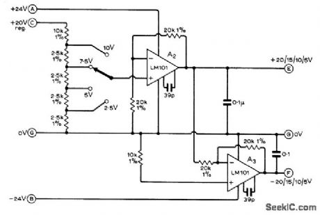
Reference voltage selected by switch is applied to noninverting input of opamp having voltage gain of 2, to provide both positive and negative regulated voltages at desired value, Any standard opamp, such as μA709 or μA741,can be used in place of National LM101.-T. D. Towers, Elements of Linear Microcircuits, Wireless World, July 1971, p 342-346. (View)
View full Circuit Diagram | Comments | Reading(635)
4_h_SEQUENTIAL_TIMER
Published:2009/7/12 22:32:00 Author:May

Use of N8281 divider network between sections of 556 dual time gives extremely long timedelays without costly large low-leakage capacitors. First section operates as oscillator having period of 1/f. Oscillator output is applied to divide-by-/N network to give output with period of N/f for triggering second half of timer. Connection of divider to second section determines amount of delay introduced by divider. Cascading of additional dividers increases maximum delay to days or even weeks.- Signetits Analog Data Manual, Signetics, Sunnyvale, CA, 1977, p 724. (View)
View full Circuit Diagram | Comments | Reading(991)
DELAYED_PULSE_GENERATOR
Published:2009/7/16 22:07:00 Author:Jessie

This circuit produces a delayed pulse width of 1.1(Rt2Ct2). The delay is given by T=1.1(Rt1Ct1). A 556 dual timer can be used. (View)
View full Circuit Diagram | Comments | Reading(4111)
SIMPLE_PULSE_STRETCHER
Published:2009/7/16 22:06:00 Author:Jessie

A single gate (open collector, noninverting) produces a simple one-shot to produce a pulse thatstretches equal to the pulse duration,plus the R1C1 time constant. R2 is a pull-up resistor to keep thegate's input high while waiting for a pulse. (View)
View full Circuit Diagram | Comments | Reading(1533)
Constant voltage and constant current regulated power supply circuit diagram
Published:2011/7/20 5:15:00 Author:nelly | Keyword: Constant voltage, constant current, regulated power supply

View full Circuit Diagram | Comments | Reading(5361)
FAST_LOW_DUTY_CYCLE_PULSE_OSCILLATOR
Published:2009/7/16 22:05:00 Author:Jessie

This simple and symmetrical free-running generator has a 50-Ω output impedance, a pulse width of 100 ns and complementary outputs that swing essentially from ground to the power-supply voltage. Moreover, it functions with a power supply range from < 1 to > 15 V and maintains a low voltage and temperature drift while consuming little power.
For oscillation to occur, each transistor must have a gain greater than unity. This restricts the value of R to a range of 1 kΩ to 1 MΩ, because the gain will be less than unity when the transistor is saturated or when beta is low as a result of small collector currents. The two RC timing networks do not have to match because the RC with the longest time constant will determine the frequency of oscillation. (View)
View full Circuit Diagram | Comments | Reading(814)
ELECTROMAGNETIC_LEVITATOR
Published:2009/7/16 22:04:00 Author:Jessie
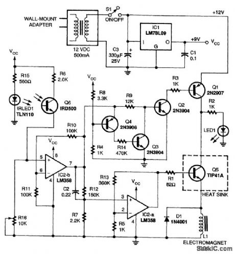
This circuit is used to levitate a steel ball as a demonstration of levitation via an electromagnet. An infrared photodetector is used to sense the position of a steel ball and control the current in the electromagnet via a feedback loop. An infrared emitter and detector mounted across from each other create an invisible beam that passes slightly below the coil. As the object rises toward the electro-magnet, it begins to block the beam. When the beam becomes blocked, the output of the detector is reduced, which, in turn, reduces the current in the electromagnet's coil. The reduced current weakens the magnetic field, the object begins to drop, and the detector once again sees more of the beam.This causes the circuit to increase the magnetic field, and the cycle repeats as the object is attracted upward again. The circuit is designed go that eventually an equilibrium is reached where the magnetic attraction exactly balances the force of gravity pulling on the object. The object then remains perfectly suspended in the infrared beam's path with no visible means of support! (View)
View full Circuit Diagram | Comments | Reading(1871)
555_PULSE_GENERATOR
Published:2009/7/16 22:04:00 Author:Jessie

This approach to using a NEC555 timer uses two diodes to set the charge and discharge timer of capacitor, which gives the circuit a variable duty factor. (View)
View full Circuit Diagram | Comments | Reading(3142)
POSITIVE_PULSE_PULSE_STRETCHER
Published:2009/7/16 22:03:00 Author:Jessie
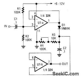
A simple pulse stretcher built with two sections of an op amp uses voltage follower U1A to drive D1 and C2. C2 charges to the peak value of pulse voltage. R3 and R4 determine the discharge time of C2 and therefore the pulse stretching. U1B acts as a voltage follower. Typically this circuit can stretch a pulse by a factor of 50. C2 can be charged to accommodate different pulse rates. (View)
View full Circuit Diagram | Comments | Reading(2678)
STABLE_START_STOP_OSCILLATOR
Published:2009/7/16 22:03:00 Author:Jessie

Oscillators that generate a predetermined number of pulses are often required in applications such as video work. This oscillator starts 13 ms after the control signal goes high and stops immediately when the input signal goes low. (View)
View full Circuit Diagram | Comments | Reading(813)
FREE_RUNNING_PULSE_GENERATOR
Published:2009/7/16 22:02:00 Author:Jessie
C1 alternately charges vla R1/D1 charges vla R2, which produces a dutyabout 1∶60. (View)
View full Circuit Diagram | Comments | Reading(487)
KEYING_CIRCUIT
Published:2009/7/16 22:02:00 Author:Jessie
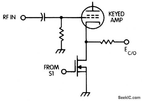
A power MOSFET can cathode-key a high-power RF amplifier. (View)
View full Circuit Diagram | Comments | Reading(680)
FLASH_MEMORY_PROGRAMMER
Published:2009/7/16 22:01:00 Author:Jessie
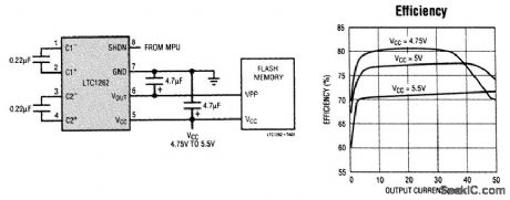
Generating 12V from a 5-V supply for flash memory usually requires a switching regulator and inductor to produce the necessary 30-rnA byte-wide flash. The LTC1262 reduces to just four small capacitors and no inductors the components required for this dc-to-dc conversion function, which generates 30 mA guaranteed output current from a 5-V ±5 percent supply. This surface-mount solution requires less than 0.2 in2. The LTC1262 features a charge-pump-gated oscillator/tripler architecture operating at 300 kHz. The gating of the oscillator regulates the output voltage at 12V.Operating supply current for the LTC1262 is 1 mA maximum, which drops just 10μA max when the device is shut down. Output voltage ramp-up is well behaved, with absolutely no overshoot. The LTC1262 is specified to operate with input voltages down to 4.75 V and up to 5.5V. (View)
View full Circuit Diagram | Comments | Reading(725)
TRANSISTOR_PULSE_GENERATOR
Published:2009/7/16 22:01:00 Author:Jessie

Seven-V narrow pulses from 2 Hz to 50 kHz are produced by this circuit. C1 through C4 provide frequency ranges in decode steps. R1 and R2 control the charging time of C1 through C4. R2 is a potentiometer used to set the frequency. R8 controls pulse width. Pulse width varies from 7 μs to 10 ms. Depending on the frequency, R8 can be deleted if it is not needed. (View)
View full Circuit Diagram | Comments | Reading(1083)
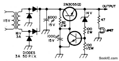
SPLIT_12_V_POWER_SUPPLY
Published:2009/7/16 22:01:00 Author:Jessie
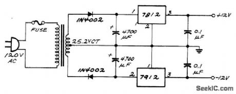
Two IC regulators and a bridge circuit supply ±12 V. (View)
View full Circuit Diagram | Comments | Reading(2378)
DUAL_SUPPLY
Published:2009/7/16 22:00:00 Author:Jessie
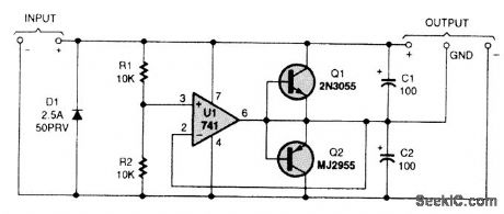
The key idea is that in a dual-supply powered circuit, ground is midway between the positive and negative supply voltages. Unfortunately, ordinary voltage regulators can't do the job. The reason is that they cart only source current, not sink it, and the ground terminal in a dual supply might have to either source or sink current, depending on which half of the load is drawing more current at the time. In the circuit, R1 and R2 divide the input voltage in half. Op amp U1 reproduces that voltage at the ground output terminal by making either Q1 or Q2 conduct as much as necessary. Capacitors Ct and C2 hold the output voltage steady when the load changes suddenly. Diode D1 is present to protect the circuit's input from reversed polarity by blowing the fuse of the main power supply. If your power supply has no fuse, place D1 in series with the circuit. That will afford the same protection with only slightly reduced regulation and voltage output. (View)
View full Circuit Diagram | Comments | Reading(1565)
LOW_POWER_RING_COUNTERLESS_THAN_6_mW
Published:2009/7/16 22:00:00 Author:Jessie
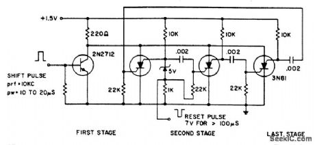
The ring counter operates from 1.0 to 6.0 V and requires only 6 mW at 1.5 V. The reset pulse turns on the first stage with its trailing edge. The maximum shift pulse width increases with voltage and approaches 70 μs for a 6.0-V supply. Minimum pulse width is 10 μs. (View)
View full Circuit Diagram | Comments | Reading(595)
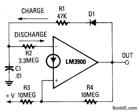
NEGATIVE_PULSE_STRETCHER
Published:2009/7/16 21:59:00 Author:Jessie

U1A acts as an amplifier, which drives D2 and charges C2. U1B acts as a voltage follower. R3 and R4 determine the amount of stretch that the input pulse receives. C2 can be charged to accommodate different pulse rates. (View)
View full Circuit Diagram | Comments | Reading(607)
INEXPENSIVE_PULSE_GENERATOR_FOR_LOGIC_TROUBLESHOOTING
Published:2009/7/16 21:58:00 Author:Jessie

Built around a 555 timer IC, this pulse generator can be built into a probe for logic troubleshooting. R11 is frequency controlled and gives a range of about 5 to 200 Hz. C2 can be reduced for higher frequencies. S2 selects one shot or pulse operators. Q1 and Q2 provide a fast rise-time pulse, which acts as a clipper amplifier. Q4 acts as a regulator. The supply can be anything from about 4.5 to 18 Vdc. LED1 is an indicator that shows circuit operation. (View)
View full Circuit Diagram | Comments | Reading(987)
12_V_FOR_TRANSCEIVER
Published:2009/7/16 21:58:00 Author:Jessie
Permits operation of 144-MHz transceiver from AC line at base station. If 18-V transformer at 3 A is not available, use 12-V 3-A unit and add 26 turns No. 20 tefloncoated wire to secondary in proper phase. Choose transformer having enough room for these extra turns.-W. W. Pinner, Midland 2 Meter Base or Portable, 73 Magazine, Aug. 1974, p 61-63. (View)
View full Circuit Diagram | Comments | Reading(633)
| Pages:746/2234 At 20741742743744745746747748749750751752753754755756757758759760Under 20 |
Circuit Categories
power supply circuit
Amplifier Circuit
Basic Circuit
LED and Light Circuit
Sensor Circuit
Signal Processing
Electrical Equipment Circuit
Control Circuit
Remote Control Circuit
A/D-D/A Converter Circuit
Audio Circuit
Measuring and Test Circuit
Communication Circuit
Computer-Related Circuit
555 Circuit
Automotive Circuit
Repairing Circuit