
Circuit Diagram
Index 756
Pulse width modulation circuit (555)
Published:2011/8/4 8:29:00 Author:nelly | Keyword: Pulse width, modulation

(a) circuit diagram (2)waveform (View)
View full Circuit Diagram | Comments | Reading(673)
Alternately change polarity pulse width modulator circuit (555)
Published:2011/8/4 8:43:00 Author:nelly | Keyword: change polarity, pulse width, modulator

(a)circuit diagram (b)waveform
Note:measuring the voltage waveform at the two ends of PR2 can know the waveform and amplitude of input current. (View)
View full Circuit Diagram | Comments | Reading(1532)
Pull-push switch circuit diagram
Published:2011/7/20 5:29:00 Author:nelly | Keyword: Pull-push switch

As shown in the figure, it is the pull-push switch circuit which is composed of P channel and channel power MOSFET transistor, it does not require bootstrap circuit.
(View)
View full Circuit Diagram | Comments | Reading(734)
Advanced drive circuit diagram
Published:2011/7/20 5:34:00 Author:nelly | Keyword: drive

As shown in the figure, it is the advanced drive circuit which is composed of P channel power MOSFET, one terminal of the load is ground connection, it does not require bootstrap circuit, so it is mainly used in lower voltage switch circuit.
(View)
View full Circuit Diagram | Comments | Reading(528)
TUNNEL_DIODE_LEVEL_DISCRIMINATOR
Published:2009/7/16 22:41:00 Author:Jessie

Tunnel diode at input of high-gain amplifier stage gives highly accurate trigger action even for slowly rising input pulse. Used with quinary scalers to measure time intervals accurately to within 1 nsec.-R. Englemann, Quinary Scalers: Measure Time Intervals Digitally, Electronics, 37:5, p 34-36. (View)
View full Circuit Diagram | Comments | Reading(734)
BASIC_FORWARD_CONVERTER_CIRCUIT
Published:2009/7/16 22:38:00 Author:Jessie

The figure is a simplified schematic for a transformer-coupled forward converter. Based on the buck converter, it is similar to the flyback converter. Inductor L1, rather than transformer T1, stores the energy. When switching transistor Q1 turns on, current builds in the primary winding of trans-former T1, storing energy. Because the secondary winding has the same polarity as the primary winding, energy is transferred forward to the output. Energy is also stored in inductor L2 through forward-biased diode D2. At this time, flywheel diode D3 is back-biased. When Q1 turns off, the transformer winding voltage reverses, back-biasing diode D2. Diode D3 becomes forward-biased, causing current to flow through RL and delivering energy to the load through inductor L1. The third winding and diode Dl return transformer T1's magnetic energy to the dc input when Q1 is off. (View)
View full Circuit Diagram | Comments | Reading(1447)
FEEDBACK_AMPLIFIER_INTEGRATOR
Published:2009/7/16 22:38:00 Author:Jessie
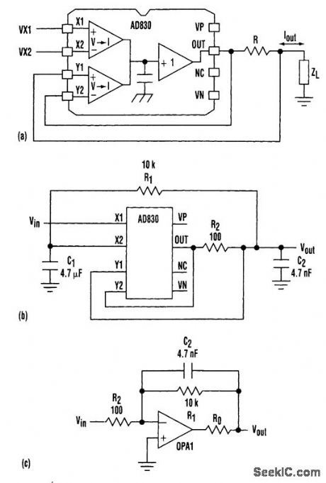
The active-feedback-amplifier topology, such as that in the AD830 from Analog Devices and Lin-ear Technology's LTC1193, can be used to produce a precision voltage-to-current converter. This, in turn, makes possible the creation of grounded-capacitor integrators. This circuit can be used as a differential input integrator by making ZL a capacitor. Figure 1b and 1c compares the grounded-capacitor integrator using the AD830 with a standard op-amp integrator. R1 in both figures and C1 in Fig.16 define the dc operating point for testing purposes. R2 and C2 determine the integrator time constant. If the op amp in Fig.1c is ideal in the sense that it is modeled as an ideal integrator with zero output and infinite input resistance, then the only difference between the two circuit topologies is the finite input resistance of the op-amp circuit determined by R2.
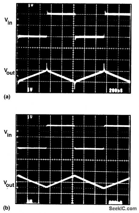
A large spike is produced on the output voltage waveform whenever the input switches using the circuit with the standard op-amp integrator (a). The integrator using the AD830 has no spike in its output waveform because the capacitor is connected to a true ground (b). (View)
View full Circuit Diagram | Comments | Reading(1403)
TUNNEL_DIODE_DISCRIMINATOR
Published:2009/7/16 22:38:00 Author:Jessie

Td1, biased dose to its peak current, is connected to d-c amplifier to overcome inherent limitations of tunnel diode. When input voltage makes current through R3 exceed diode peak current, diode switches to its high-voltage state of 0.5 v. Q1 amplifies this change by factor of 10, and Q2 initiates start of square wave output. When input drops, circuit and diode revert to original state. Rise and fall times are about 10 nsec.-G. Marosi, Versatile Tunnel-Diode Discriminator, FEE, 14:5, p l20. (View)
View full Circuit Diagram | Comments | Reading(714)
125_TO_37_V_AT_15_A_
Published:2009/7/16 22:37:00 Author:Jessie

Adjustable positive voltage regulator used with simple bridge rectifier and capacitor-input filter delivers wide range of regulated voltages, all with current and thermal overload protection. Load regulation is about 0.3%.-H. Berlin, A Simple Adjustable IC Power Supply, Ham Radio, Jan. 1978, p 95. (View)
View full Circuit Diagram | Comments | Reading(956)
FIVE_OUTPUT_CONVERTER
Published:2009/7/16 22:37:00 Author:Jessie

Digital panel meters (DPMs) make excellent displays for instruments and test equipment, but they suffer from one major flaw: They require a floating power supply, usually in the form of a 9-V battery. This circuit powers up to five meters from a single 1.8- to 6-V source. Each of the five outputs is fully floating, isolated, and independent in every respect. The converter is based on a flyback design, and it uses a micropower, high-efficiency regulator (LT1303) and an off-the-shelf, surface-mount inductor. The coil has six identical windings and is high-voltage-tested to 500 V rms-more than adequate isolation for the application. Operation is as follows: Feedback is extracted from the primary by Q1, which samples the flyback pedestal during the switch-off time. Typical DPMs draw approximately 1-mA supply current. The primary also is loaded with 1 mA for optimum regulation and ripple. Snubbing components, a necessity in most flyback circuits, are obviated by the action of C1 and C2. The converter also can be used with a battery. In this case, a sixth panel meter can be powered by the primary across C2. All that is required to balance the load current is to increase R1 and R2 by a factor of 10. Although this circuit is set up for 9-V output (actually 9.3 V), some DPMs need 5 or 7 V. As a result, a 4.3- or 6.2-kΩ resistor should be used in place of R1 for these voltages. The output voltage is set by R1 = (Vout-0.7)/1 mA. If any outputs aren't needed, omit the associated components and parallel the unused winding with the primary, observing the phasing. With each output loaded at 1 mA, the input current is 16.5 mA on a 5-V supply. This figure rises to about 45 mA on a 1.8-V (two-cell) input. (View)
View full Circuit Diagram | Comments | Reading(874)
VOLTAGE_LIMIT_DETECTOR
Published:2009/7/16 22:36:00 Author:Jessie


Consists of two voltage dividers that set the levels between which ramp generators should remain in roster that shows computer memory performance under marginal drive currents by plot ting schmoo curves. Npn transistors ore 2N706, pnp transistors are 2N1132, and diodes are 1N921.-J. E. Gersbach, The Great Schmoo Plot: Testing Memories Automatically, Electronics, 39:15, p. 127-134. (View)
View full Circuit Diagram | Comments | Reading(1129)
BACKUP_SUPPLY_CAPACITOR
Published:2009/7/16 22:35:00 Author:Jessie

These connections allow dual control of the buffered RESET line and extend the duration of resets issued by the μP. The parts shown are CMOS RAM. (View)
View full Circuit Diagram | Comments | Reading(540)
FAST_AMPLIFIER_FOR_RANDOM_TELEGRAPH_WAVE
Published:2009/7/16 22:34:00 Author:Jessie
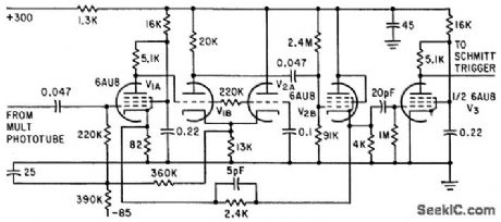
Amplifies small pulses above thresh-old value without being overloaded by large pulses derived from radioactive isotope and phosphor on envelope of multiplier photo-tube. Two feedback loops, similar to Oak Ridge-Fairstein and Brookhaven-Chase circuits, help to stabilize gain.-J. B. Manelis, Generating Random Noise with Radioactive Sources, Electronics, 34:36, p 66-69. (View)
View full Circuit Diagram | Comments | Reading(587)
ONE_IC_TRANSMIT_TONE_ENCODER
Published:2009/7/16 22:34:00 Author:Jessie
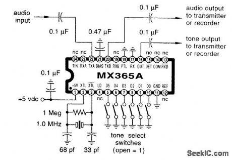
This circuit can be used in a communications transmitter or repeater to place an encoding tone on an audio signal. (View)
View full Circuit Diagram | Comments | Reading(541)
HF_AMPLIFIER_GROUNDING_TECHNIQUE
Published:2009/7/16 22:32:00 Author:Jessie
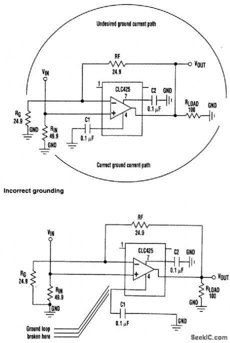
Incorrect grounding on a high-frequency amplifier allows the addition of polarized signal back into the input. Improved grounding is provided by common grounds at the input, physical orientation of a bypass capacitor, and breaking a ground loop. (View)
View full Circuit Diagram | Comments | Reading(691)
80_V_AT_15_A_FOR_COLOR_TV
Published:2009/7/17 0:13:00 Author:Jessie

Holds output voltage across RL within 2% over line-voltage range of 105 to 140 V. Designed for use in 19-inch color TV receiver having 700-V fly back horizontal system. Bridge rectifier has two 2N4442 SCRs that control amount of output voltage by using variable duty cycle. Regulator uses MPU131 programmable UJT, which also serves for gating SCRs. 1K pot provides control of PUT gate voltage, which in turn determines output voltage across RL.-R. J. Valentine, A Low-Cost 80 V-1.5 A Color TV Power Supply, Motorola, Phoenix, AZ, 1974, AN-725, p 2. (View)
View full Circuit Diagram | Comments | Reading(684)
12_V_AT_1_A
Published:2009/7/17 1:16:00 Author:Jessie

Simple supply furnishes up to 1 A with excellent regulation. Bottom of chassis can be used for heatsink. Connect additional 0.1-μF capacitor between pin 1 of VR1 and ground. T1 is Radio Shack 273-1505 with 12.6-V CT 1.2-A secondary, and F1 is 0.5-A fuse.-A. Pike, Radio Shack Power Supply, CQ, Sept.1977, p 66. (View)
View full Circuit Diagram | Comments | Reading(1014)
±0_TO_15V_AT_200mA_AND_38_TO_5V_AT_2A
Published:2009/7/17 0:11:00 Author:Jessie

Developed for use with slow-scan television. Design provides equal positive and negative voltages that track each other with one manual control, adjustable from 0 to 15 V for opamps. Current limiting is provided for both positive and negative outputs. Low digital voltage can be adjusted to 3.8 V for RTL or 5 V for TTL, without current limiting. Use transformer having 35-V secondary, center-tapped, rated at 3 A.-D. Miller and R. Taggart, Popular SSTV Circuits, 73 Magazine, March 1973, p 55-60, 62, and 64-67. (View)
View full Circuit Diagram | Comments | Reading(923)
±115_V
Published:2009/7/17 0:09:00 Author:Jessie

Developed for experimentation with IC audio amplifiers, delivering up to 5 W, where good regulation is required to prevent oscillation caused by feedback through power supply to input stage. Q1 and Q2 are inexpensive silicon transistors, serving also as low-cost fuse because they burn out first when power supply is overloaded. Use heatsinks with silicone grease for output transistors.-D. J. Kenney, Integrated Circuit Audio Amplifiers, 73 Magazine, Feb. 1974, p 25-30. (View)
View full Circuit Diagram | Comments | Reading(742)
ACTIVE_HIGH_Z_PROBE
Published:2009/7/16 23:52:00 Author:Jessie

This probe has a 100 mΩ input impedance and uses a T1 TLC2254 quad op amp operating from a 12 V battery.It can be used with a DVM or an analog multimeter for measurments in the high-impedance circuits. BP1 is a Tellon standoff to ensure low leakage t the terminal. (View)
View full Circuit Diagram | Comments | Reading(2714)
| Pages:756/2234 At 20741742743744745746747748749750751752753754755756757758759760Under 20 |
Circuit Categories
power supply circuit
Amplifier Circuit
Basic Circuit
LED and Light Circuit
Sensor Circuit
Signal Processing
Electrical Equipment Circuit
Control Circuit
Remote Control Circuit
A/D-D/A Converter Circuit
Audio Circuit
Measuring and Test Circuit
Communication Circuit
Computer-Related Circuit
555 Circuit
Automotive Circuit
Repairing Circuit