
Circuit Diagram
Index 745
VOLTAGE_CONTROL_OF_ASTABLE_MVBR
Published:2009/7/16 22:18:00 Author:Jessie

Addition of two transistors to basic astable mvbr gives voltage-controlled constant-duty-cycle variable-frequency operation. Frequency range is 210 cps to 210 kc, ratio of 1,000 to 1, with less than 5% departure from linearity with change in control voltage.-W. J. Mattox, A Versatile, Very-Wide Range Multivibrator, EEE, 13:7, p 59-61. (View)
View full Circuit Diagram | Comments | Reading(736)
UJT_MVBR
Published:2009/7/16 22:16:00 Author:Jessie

Unijunction transistor serves as multivibrator, with Q2 amplifying its output and providing isolation from load.-F. W. Kear, Unijunction Transistor Pulse-Circuit Design, Electronics, 35:21, p 58-60. (View)
View full Circuit Diagram | Comments | Reading(734)
PIN_DIODE_SWITCH_AND_ATTENUATOR_CIRCUIT
Published:2009/7/16 22:15:00 Author:Jessie

This circuit is a basic PIN-diode switch building block. R1 is chosen from Idiode=(Vcc-Vdiode)/(R1+R2) ,where Idiode is the specified diode current. (View)
View full Circuit Diagram | Comments | Reading(725)
400_CPS_UJT_MVBR
Published:2009/7/16 22:15:00 Author:Jessie

Off time is determined primarily by R1, and on time primarily by R2. Frequency is inversely proportional to size of capacitor.- Transistor Manual, Seventh Edition, General Electric Co., 1964, p 340. (View)
View full Circuit Diagram | Comments | Reading(548)
±15_V_100_mA_DUAL_POWER_SUPPLY
Published:2009/7/16 22:13:00 Author:Jessie

A simple supply such as this is useful for many small projects, op amp circuits, etc. (View)
View full Circuit Diagram | Comments | Reading(912)
1_CPS_250_KC_ASTABLE_MVBR
Published:2009/7/16 22:13:00 Author:Jessie

Used as free-running oscillator for generating square waves and timing frequencies, and for frequency division. Synchronizing pulses permit generation of subharmonics. Sync pulse amplitude must exceed +1.5 V with rise time less than 1 microsec.- Transistor Manual, Seventh Edition, General Electric Co., 1964, p 201. (View)
View full Circuit Diagram | Comments | Reading(601)
DUAL_OUTPUT_VOLTAGE_REGULATOR
Published:2009/7/16 22:13:00 Author:Jessie

The LTC1266-3.3 and the LTC1263 are perfect complements for one another. The combination of the two parts provides two regulated outputs of 3.3 V/5 A and 12 V/60 mA from an input range of 4.75 to 5.5 V. The LTC1263, using only four external components (two 0.47-μF charge capacitors, one 10-μF bypass capacitor, and one 10-μF output capacitor), generates the regulated 12-V/60-mA output from a 5-V input using a charge-pump tripler. During every period of the 300-kHz oscillator, the two charge capacitors are first charged to VCC and then stacked in series, with the bottom plate of the bottom capacitor shorted to VCC and the top plate of the top capacitor connected to the output capacitor. As a result, the output capacitor is slowly charged up from 5 to 12 V. The 12-V output is regulated by a gated oscillator scheme that turns the charge pump on when Vout is below 12 V and turns it off when it exceeds 12 V. The LTC1266-3.3 then uses the 5-V input, along with the 12-V output from the LTC1263 and various external components, including bypass capacitors, sense resistors, and Schottky diodes, to switch two external N-channel MOSFETs and a 5-μH inductor to charge and regulate the 3.3-V/5-A output. The charging scheme for this part, however is very different from that of the LTC1263. The LTC1266-3.3 first charges the output capacitor by turning on the top N-channel MOSFET, allowing current to flow from the 5-V input supply through the inductor. The amount of current flow in the inductor is monitored with a sense resistor, and the 3.3-V output is regulated by turning on and off the top and bottom N-channel MOSFETs to charge and discharge the output capacitor. (View)
View full Circuit Diagram | Comments | Reading(941)
SINGLE_POT_SWINGS_AMPLIFIER_GAIN_POSITIVE_OR_NEGATIVE
Published:2009/7/16 22:12:00 Author:Jessie
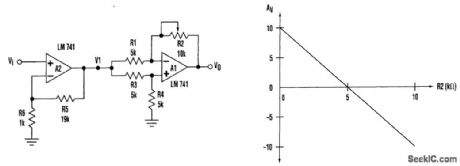
It is handy to have a gain block with a gain that can be varied smoothly from positive to negative with a single potentiometer. The circuit shown accomplishes this function with R2. Op amp A1 is configured with both inputs tied together. Op amp A2 functions as a buffer. WithR1=R3=R4=R=5KΩ,the gain of the differential amplifier is given by AV1=(V0/V1)=1/2(1-R2/R). With a buffer amplifier gain of 20, the overall gain of the amplifier is given by AV=(V0/V1)=10(1-R2/R). By using a 10-turn potentiometer, the gain can be varied from positive to negative. (View)
View full Circuit Diagram | Comments | Reading(712)
DUAL_5_V
Published:2009/7/16 22:10:00 Author:Jessie

Provides two 5-V regulated supplies for frequency counter, operating either from 9-VDC outputs of AC supply or from 12-VDC auto battery. Splitting of supply divides current demand so regulators operate well below maximum ratings and provide decoupling between sections of load.-J. Pollock, Six Digit 50-MHz Frequency Counter, Ham Radio, Jan. 1976, p 18-22.
(View)
View full Circuit Diagram | Comments | Reading(924)
DELUXE_RADAR_DETECTOR_
Published:2009/7/16 22:10:00 Author:Jessie

This simple radar detector includes an audio amplifier for driving a loud speaker. As in Fig. 69-1, it uses an op amp as a detector of microwave signals. (View)
View full Circuit Diagram | Comments | Reading(4593)
Transistor tracking regulated power supply circuit diagram
Published:2011/7/20 5:14:00 Author:nelly | Keyword: Transistor, tracking, regulated power supply

As shown in the figure, it is the transistor tracking regulated power supply circuit, the input voltage is ±24V, the output voltage is 0~+15V and 0~-15V, the maximum output current is 3A.
(View)
View full Circuit Diagram | Comments | Reading(3212)
SCR_LAMP_BRIGHTNESS_CONTROL
Published:2009/7/12 22:37:00 Author:May

Will control up to 1.6 amp rms while operating directly from power line, yet is sufficiently compact to fit into base of common household lamp socket.-Low-Cost, Low-Power SCR's to invade Commercial Market, EEE, 13:8, p21-22. (View)
View full Circuit Diagram | Comments | Reading(642)
LIQUID_DENSITY_GAGE
Published:2009/7/12 22:36:00 Author:May
Peltier-effect semi-conductor thermoelements maintain uniform cooling temperatures required for accurate specific gravity measurements. Null-position detecting circuit uses differential transformer to sense position of movable core at end of float.-C. W. Hargens, Semiconductors Cool and Control Density Gage, Electtonics, 31:49, p 80-8l. (View)
View full Circuit Diagram | Comments | Reading(1018)
800_W_TRIAC_DIMMER
Published:2009/7/12 22:34:00 Author:May
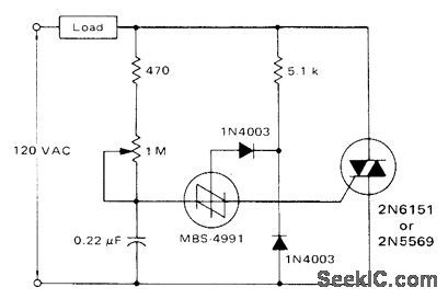
Simple circuit uses Motorola MBS-4991 silicon bilateral switch to provide phase control of triac. 1-megohm pot varies conduction angle of triacfrom0o to about 170o, to give better than 97% of full power to load at maximum setting. Conduction angle is the same for both half-cycles at any given setting of pot.-- Circuit Applications for the Triac, Motorola, Phoenix, AZ, 1971, AN-466 p 5. (View)
View full Circuit Diagram | Comments | Reading(1853)
LINEAR_DAC_WITH_NONLINEAR_OUTPUT
Published:2009/7/12 22:34:00 Author:May
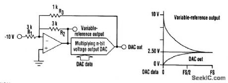
When controlling a nonlinear device, such as an incandescent lamp, it is desirable to have fine resolution at the high end, where a small change in current can cause a large change in brightness.At the low end, coarser resolution is quite adequate. Using the circuit shown, any desired compression can be produced using just about any multiplying DAC. A negative 10-V reference is fed through R1 to inverting amplifier A1, which has an initial gain set to unity by R2. A1's output supplies a positive variable reference to the DAC. The DAC output provides additional feedback through R3, reducing the amplifier's gain as the DAC data increase. The variable reference is gradually reduced so that each step is progressively smaller than the one before. With the values shown, as the DAC data approaches full-scale; the reference approaches 1/4 of its original value. This produces output with four times as much resolution at the high end as at the low end. By decreasing the value of R3, greater compression and higher resolution can be achieved. The variable-reference output also can be useful in some applications. (View)
View full Circuit Diagram | Comments | Reading(758)
15_V_FOR_VTVM
Published:2009/7/12 22:33:00 Author:May

Simple rectifier circuit replaces battery in vacuum-tube voltmeter. Provides good regulation and eliminates need for frequent battery replacement. Remove battery before using supply. AC source can be 6.3-V secondary of filament transformer or terminals of 6.3-V pilot lamp in any AC equipment.-P. Alexander, Battery Replacement Circuit for VTVM, QST, Jan. 1976, p 42-43. (View)
View full Circuit Diagram | Comments | Reading(748)
DIGITAL_LOCK_CIRCUIT
Published:2009/7/12 22:33:00 Author:May

This circuit depends on the entry of a correct sequence code. An incorrect number that is not part of the code causes the circuit to reset. When the correct code is entered, Q2 operates relay K1 for a short time, depending on C3. (View)
View full Circuit Diagram | Comments | Reading(1814)
±4_V_TO_±25_V
Published:2009/7/16 22:09:00 Author:Jessie

Arrangement permits varying both positive and negative regulated output voltages simultaneously with single control, with maximum load current of 400mA for both regulators. Positive supply controls negative slave regulator to provide tracking within 0.05 V at full output. Developed for use in lab to observe effect of varying supply voltages on circuits under development. -J. A. Agnew, Dual Power Supply Delivers Tracking Voltages, EDN Magazine, Oct.15, 1970, p 51. (View)
View full Circuit Diagram | Comments | Reading(1945)
RADAR_DETECTOR
Published:2009/7/16 22:09:00 Author:Jessie
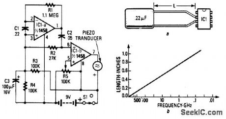
A simple detector of radar signals uses the junctions of the input transistors of an LM1458 op amp as RF detectors. The leads of C1 act as an antenna and should be about 0.4 long measured from the IC package. Detected audio components are further amplified by IC1A and IC1B, and drive a piezo transducer. Mount the circuit so that incident RF energy will not be blocked. (View)
View full Circuit Diagram | Comments | Reading(2966)
The application circuit diagram of S812/S802 series regulator
Published:2011/7/20 5:19:00 Author:nelly | Keyword: regulator
View full Circuit Diagram | Comments | Reading(822)
| Pages:745/2234 At 20741742743744745746747748749750751752753754755756757758759760Under 20 |
Circuit Categories
power supply circuit
Amplifier Circuit
Basic Circuit
LED and Light Circuit
Sensor Circuit
Signal Processing
Electrical Equipment Circuit
Control Circuit
Remote Control Circuit
A/D-D/A Converter Circuit
Audio Circuit
Measuring and Test Circuit
Communication Circuit
Computer-Related Circuit
555 Circuit
Automotive Circuit
Repairing Circuit