
Circuit Diagram
Index 761
RESET_MODE
Published:2009/7/12 21:41:00 Author:May

RCA CA555 timer is connected so CT is initiallyheld in discharged stata bytransistor in IC. When start switch is closed, internal flip-flop clears short across CT, driving output voltage high and energizing relay. Voltage across capacitor then increases exponentially with time constant R1CT. When capacitor voltage equals two-thirds of V+, flip-flop resets and discharges capacitor rapidly, driving output low and releasing relay. Timing interval is relatively independent of supply voltage variations. Applying negative pulse simultaneously to reset pin 4 and trigger pin 2 by closing both switches during timing cycle causes timing cycle to restart. Momentary closing of reset switch only serves to discharge CT without restarting timer. - Linear Integrated Circuits and MOS/ FET's, RCA Solid State Division, Somerville, NJ, 19-l7, p 56. (View)
View full Circuit Diagram | Comments | Reading(655)
RS232_TEST_CIRCUIT
Published:2009/7/12 21:40:00 Author:May

The tester is basically a window comparator, in which the low and high levels are set at +3.0 V and -3.0 V, respectively, by resistors R2, R3, and R4. Resistor R1, when not driven by an RS232 output, will have a low voltage across it (approximately 0 V), and the LED D1 at the output of the comparators is turned off. If the unknown wire of the cable that is tested is an RS232 output, then it will drive the in point to avoltage either between +3 and +12Vor between -3 and -12 V. In both cases, one of the two comparator outputs will be driven low. This turns the LED on, indicating the presence of a wire connected to an,RS232 output. The comparator should be an LM339 type or equivalent (with an open-collector output). The disadvantage of this scheme is that the thresholds are very sensitive to the supply variations. To eliminate this problem, the thresholds at the inputs of the comparators can be created using the normal forward drop on a simple diode and then be brought to the necessary leyels by IC1 (+3 V at its output) and IC2 (a simple inverter). (View)
View full Circuit Diagram | Comments | Reading(1826)
WINDOW_COMPARATORS
Published:2009/7/12 21:39:00 Author:May

In Fig. 104-3(a), when YIN is between reference voltages VL and VU, output VOUT goes low. If VIN >VL IC2 produces a low. Because IC1 outputs low, if VIN>VU, both outputs are low and VOUT is low. If VIN<VL both IC1 and IC2 are low. Figure 104-3(b) operates the reverse of this; it produces a high when VL<VIN < VU. (View)
View full Circuit Diagram | Comments | Reading(697)
BATTERY_SWlTCH_OFF
Published:2009/7/12 21:39:00 Author:May

Can be added to any battery-operated device to eliminate unnecessary running down of costly batteries when someone forgets to tum switch off manually. Circuit shown gives operating time of about 10 hours ,permitting use of equipment for full working day without interruption. Normal operation can be restored after shut-off byturning manual switch off and then on again. When circuit has switched off, only battery drain is current through 10-megohm resistor R1 and leakage through transistors. Time of switch-off can be changed by altering C2 or R7. Tr1 and Tr2 are 2N4061, BC478, or similar PNP silicon; Tr3 is 2N3053, BC142, or similar medium-power NPN silicon; Tr4 and Tr5 are 2N3819; D1 is any small silicon diode; R6 is 4.7K for 9-V or 12-V battery, and 10K for 15-V to 27-V battery. R2 is chosen to suit working current and battery voltage; suitable value is 15Vb/Iout.-D, T. Smith, Automatic Battery Switch-Off Circuit, Wireless World, April 1976, p 76.
(View)
View full Circuit Diagram | Comments | Reading(1117)
THREE_WIRE_RS232_TO_RS485_CONVERTER
Published:2009/7/12 21:39:00 Author:May


This circuit needs only a minimal three-wire RS232 implementation plus one +10-to +15-V supply voltage to provide a transparent link capable of sending data at transmission rates up to tens of kbaud Circuit operation is as follows∶When both the 232 and the 485 are idle(232 port in MARK state and no 485 device active),the 485 link is held in the 1 state by the 1200-Ω pullup This causesthe top comparator to hold the 232 RCD line negative and therefore in MARK state When a character is transmitted by the 232 port,it begins with a positive-going (SPACE state) START bit on the TXD line,In response, the 2N4401 pulls the - 485 conductor more positive than the + wlre,thustransmitting the START down the 485 cable Meanwhile,the bottom comparator holds the wlre-or (LM393s have opencollector outputs)232 RCD low, blocking the ooodJt port from hearing its own transmission.The recelve side ofthe 232 port remalns idle The rest ofthe bits ofthe character follow along in the same fashion When a character originates somewhere along the 485 bus,it beginswith a 485 transceiver gong active and driving the - line above the + This causes the upper half of the LM393 comparator to release RCD,and this time the bottom comparator doesn't prevent it from being pulled high The data bits are thus allowed to arrlve at the RS232 port,where they appearat standard RS232 bipolar voltage levels,The commonmode voltage range and noise-rejection capabilities of this circuit are compatible with standard 485 specifications The converter's speed is mainly limited by the loading of the comparator outputs because of cable capacitance. (View)
View full Circuit Diagram | Comments | Reading(1670)
SENSE_AMPLIFIER_READS_MEMORY_DATA
Published:2009/7/12 21:36:00 Author:May

Small signals stored in thin-film momory are amplinfied while rejecting noise from partially selecled bits on same sense line. Circuit is completely isolated differential amplifier operating from low-impedance source.-A.A.Fleischer and E.Johnson, New Digital Conversion Method Provides Nanosecond Resolution, Electronics, 36:18, p55-57. (View)
View full Circuit Diagram | Comments | Reading(477)
AC_CONTROL_WITH_TRIAC
Published:2009/7/12 21:34:00 Author:May

Decoder outputs of microprocessor feed 7476 JK fliρ-floρ thatdrives optocoupler which triggers triac for ON/OFF control of lamp or other AC load. LED andcadmium sulfide photocell are mounted in light shield. When light fron LED is on photocell, cell resistance drops and allows control voltage of correct direction and amplitude to trigger gate of triac, turning it on. When light disappears,triac remains on until voltage falls near zero in AC cycle.-R. Wright, Utilize ASCLL Control Codes!, Kilobaud, Oct, 1977, p 80-83. (View)
View full Circuit Diagram | Comments | Reading(1425)
CASCADED_TIMER
Published:2009/7/12 21:34:00 Author:May
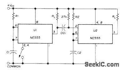
Two NE555 timers give sequential timing intervals for two separate loads.Time for U1 is set by R1 and C1, and for U2 by R2 and C2. Grounding pin 2 momentarily with switch starts timing. Once started, it cannot be retriggered. With pin 2 connected to reset input 4, both functions are obtained with one push of switch, lf reset function is not wanted, connect 4 to 8. When pin 3 of U1 goes low at end of timing interval, negative pulse generated by 0.001-μF capacitor and 27K resistor goes to pin 2 of U2 to trigger second timer. With 15-V supply, each timer can handle 200-mA load.-H. Vordenbaum, Automatic Reset Timer, Ham Radio, Oct. 1974, p 50-51. (View)
View full Circuit Diagram | Comments | Reading(956)
10s_USING_15_V_SUPPLY
Published:2009/7/12 21:33:00 Author:May
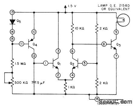
RCA CA3096E fivetransistor array drives indicator lamp thatcomes on at end of timing interval,Q5 is one of PNP transistors in array connected as diode.- Linear Integrated Circuits and MOS/FET's, RCA Solid State Division,Somerville,NJ,1977,p205-210. (View)
View full Circuit Diagram | Comments | Reading(688)
WINDOW_GENERATOR
Published:2009/7/12 21:33:00 Author:May
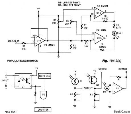
This window generator uses a single LM324 op amp and features two adjustable set points. When the two comparators formed by U1B go high, LED1 lights. When U1C goes high, the LED extinguishes. Some hysteresis is provided by the 10-mΩ resistors. As shown in Fig. 104-2(b), LED1 can be replaced by an optoisolator (etc.) for use in several applications. (View)
View full Circuit Diagram | Comments | Reading(1665)
SENSE_AMPLIFIER_AND_GATE
Published:2009/7/12 21:30:00 Author:May
Uses drive-sampling core to generate precisely defined strobe for coincident-current memory.-A.H.Ashley and E.U. Cohler,solving Noise Problems in Digital compuler Memories Electronics,33:13,p72-74. (View)
View full Circuit Diagram | Comments | Reading(459)
RS232_TO_PARALLEL_DATA_CONVERTER
Published:2009/7/12 21:28:00 Author:May


A simple serial decoder circuit based on a 6402 UART (IC1) is shown in the figure. The RS232C input signal is at signal levels of about ±12 V; these must be converted to standard 5-V logic levels before being applied to the serial input of IC1. A simple commonemitter switching stage based on transistor TR1 is used to provide the conversion to normal logic levels, and it also produces the necessary inversion of the input signal. Resistor R4 and capacitor C1 provide IC1 with a positive reset pulse at switch-on. The inputs at pins 35 to 39 program the word format; the method of connection shown in the figure provides a format on 1 start bit, 8 data bits, 1 stop bit, and no parity. Pin 34 is connected to the +5-V rati so that the binary pattem on pins 35 to 39 is loaded into IC1's control register. The decoded bytes of parallel data are available at pins 5 to 12, and pin 4 is connected to the 0 V rail so that these outputs are permanently enabled. In a stand-alone application, the tristate capability of these outputs is not of great value, but, if necessary, this facility can be utilized by applying a control signal to pin 4 of IC1. (View)
View full Circuit Diagram | Comments | Reading(2279)
LOW_COST_WINDOW_COMPARATOR
Published:2009/7/12 21:27:00 Author:May

This circuit outputs a TTL-compatible 100-μs pulse whenever the signal falls within the limits set by potentiometers and can be varied to suit the application.Op amps, E, D, and C are used with the two potentiometers to supply reference voltages, derived from a 1-V precision source, for two other op amps (A and B) configured as voltage comparators. The input signal is taken to the negative inputs of both these comparators. C is wired as a noninverting surnming amp, used to derive the higher reference voltage. Consequently, the acceptance window is set. Because the voltage across potentiometer P2 is 0.5V, the window can be set between 0 and 0.5 V above the value chosen for the lower reference value. The lower value is set by P1.The outputs from the comparators are sent to the inputs of inverting Schmitt triggers F and G. Although these triggers operate from a 5-V supply, they have an extended input-voltage range and are capable of handling the comparator's output voltage swings.The two monostables, J and K, are triggered on the rising edge of the Schmitt outputs. J and K set and reset the bistable latch formed by two NOR gates. Latch output Q controls the reset of outputmonostable L, which can only be triggered if its B input goes low, taken from the output of G, while its reset is high.From the timing diagram, when the signal input exceeds the lower reference level, the latch is set and Q goes high. When the higher reference level is exceeded, the latch is reset and Q goes low. If only the lower reference is exceeded, the latch will be set and L is triggered when G's output goes low. When both levels are exceeded, the latch is set, then reset. When G's output goes low, it won't trigger the monostable because its reset is low.The circuit, as shown, was used for a bandwidth-limited, 500- to 5000 Hz input signal with an amplitude range of ±1 V. Modifications can easily be made to cover other frequency and amplitude ranges. (View)
View full Circuit Diagram | Comments | Reading(943)
CALCULATOR_KEYBOARD_ENTRY_
Published:2009/7/12 21:25:00 Author:May

Sampling of signals from inexpensive pocket calculator gives complete data entry system for frequency synthesizer or other application requiring BCD input. Circuit includes contact bounce suppression. Automatic constant feature of TI 1256 calculator used permits storing 0.015 as fixed constant, so frequency goes up 15 kHz (channel spacing on 2 meters) each time + key is pressed.Seven-segment signal normally used for calculator display is decoded by programming 74S188 (8223) PROM, using simplified code conversion table given in article. 74175 ICs provide required demultiplexing of segment data. Articl gives construction details.-B .McNair andG Williman,Digital Keyboard Entry System,Ham Radio, Sept,1978,p 92-97.
(View)
View full Circuit Diagram | Comments | Reading(3472)
THIN_FILM_SENSE_AMPLIFIER
Published:2009/7/12 21:24:00 Author:May
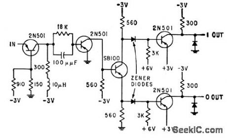
Common-base input stage matches low input impedance of sense winding. 5-mv input signal is boosted to 3-v level. Zener diodes shifl d-c levels of output signal to desired 0 to+3 v level.-E.E. Bittmann, Using Thin Films in High-Speed Memories, Electronics, 32:23, p55-57. (View)
View full Circuit Diagram | Comments | Reading(537)
WIRELESS_MICROPHONE
Published:2009/7/12 21:20:00 Author:May
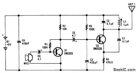
Q1 amplifies the output from an electret microphone MIC1.Audio is fed into oscillator Q2,whichmodulates the signal.LIC1 is a tank circuit for operation in the 88-MHz reglon.The antenna is a 6-to 8-inch ptece of wire.L1 is a variable inductor in the 1-μH range. (View)
View full Circuit Diagram | Comments | Reading(5465)
THIN_FlLM_CURRENT_DRIVER
Published:2009/7/12 21:20:00 Author:May
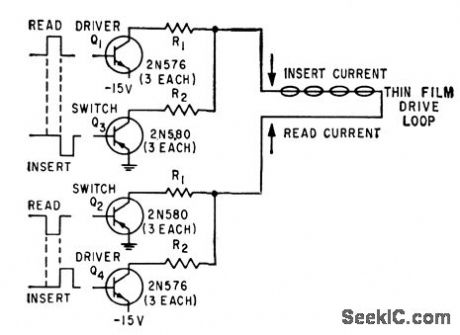
Three 2N576 driver transistors in parallel, each rated 400 ma, deliver 1-amp pulses with 0.15 microsec rise time. Three 2N580 pnp transistors in pamllel serve as current switches.-E. E. Bittmann, Using Thin Films in High-Speed Memories, Electronics,32:23,p55-57. (View)
View full Circuit Diagram | Comments | Reading(543)
WIRELESS_FM_MICROPHONE
Published:2009/7/12 21:17:00 Author:May
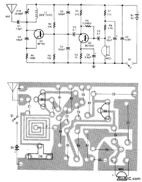
A simple FM wireless microphone uses a single BC183C transistor as an audio amplifier. A 2N3565 can be substituted. Q1 is an oscillator that is FM modulated by the signal from Q1. Other transistors can be substituted, but the modulation characteristics should be checked. (View)
View full Circuit Diagram | Comments | Reading(0)
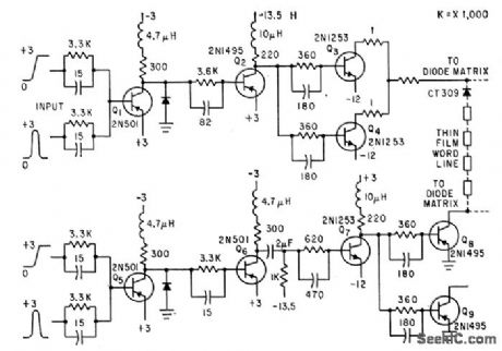
THIN_FILM_MEMORY_DRlVER
Published:2009/7/12 21:16:00 Author:May
Generales l-amp pulses with 35-nsec rise and fall times, at rates up to 1 Mc, for driving 2,560-bit memory plane using 2,000-angstrom nickeliron films.-E. E. Bittmann, Ihin Magnetic Film Memories for High-Speed Computers, Electronics, 34:9, p39-41. (View)
View full Circuit Diagram | Comments | Reading(599)
TRANSISTOR_RADIO_TURNOFF
Published:2009/7/12 21:15:00 Author:May
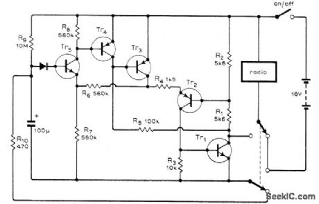
Circuit switches radio off after delay of about 30 min, if ganged switch is set to other position and radio switch itself is left on. Current drain of timer circuit is negligible in both positions. Article describes timing action of transistors in detail. Tr1 should have current gain above 25 with collectorcurrents of 10 to 100 mA; 2N3706 can be used here and for Tr5. Other transistors should have current gain above 50, as in 2N3702. For operation from 4.5 to 9 V, omit diode and cut values of R4-R7 in half.-S. Lamb, Delayed Switch Off for Transistor Radios, Wireless World, Aug. 1973, p 373. (View)
View full Circuit Diagram | Comments | Reading(945)
| Pages:761/2234 At 20761762763764765766767768769770771772773774775776777778779780Under 20 |
Circuit Categories
power supply circuit
Amplifier Circuit
Basic Circuit
LED and Light Circuit
Sensor Circuit
Signal Processing
Electrical Equipment Circuit
Control Circuit
Remote Control Circuit
A/D-D/A Converter Circuit
Audio Circuit
Measuring and Test Circuit
Communication Circuit
Computer-Related Circuit
555 Circuit
Automotive Circuit
Repairing Circuit