
Circuit Diagram
Index 770
HIGH_VOLTAGE_PROBE
Published:2009/7/17 1:56:00 Author:Jessie

This high-voltage probe allows your DMM to take high-voltage measurements to 10,000 V peak, and acts as a high-impedance (100-MΩ) probe for high-impedance circuit testing. The probe was designed to plug into a standard 10-MΩ input DMM. If your DMM has a different input, you can change R3 and R4 to suit it. The ratio of R1 + R2 + R3 + R4 should be exactly 1000 to 1; thus, a 10.00-V in-put will read 10.00 mV on your DMM. Keep in mind that the impedance of your DMM is in parallel with R3/R4 when you calculate new values. (View)
View full Circuit Diagram | Comments | Reading(3737)
PB_SWITCH_ACTIVATED_MEMORY
Published:2009/7/17 1:55:00 Author:Jessie


Many new brushless-motor control schemes use ICs that determine the rotor position by sensing the motor's back-BMP signals. In a unipolar configuration, the control chip synchronizes the three phases of drive currents by detecting the moments when each back-EMF signal rises just above, or falls just below, the motor supply voltage, VBATT (see the figure), These instances are known as zero crossings. This circuit shifts the signals down to a reference level, VREF The MOSFET, M1, along with resistor R1 and NPN transistor Q1, creates a reference current (I1) that is equal to (VBATT-VREF)/R1.This reference current is replicated in Q2, Q3, and Q4. Because R2=R3=R4=R1, the voltage drop across each resistor is the same. That means that V2,V3and V4 vary above and below VBATT the same amount as V2,V3,and V4 vary above and below VBATT Matching resistors R1 to R4 within 1 percent and matching R5 to R8 within 1 percent will resolve back-EMF signals as small as 200 mV. Diode D1 protects M1's gate from large transients on VBATT. The ESD diodes on the 551595, along with resistors R2, R3, and R4, protect the IC from damaging transients at V2,V3 and V4. (View)
View full Circuit Diagram | Comments | Reading(1801)
WIRELESS_DC_PROBE
Published:2009/7/17 1:55:00 Author:Jessie
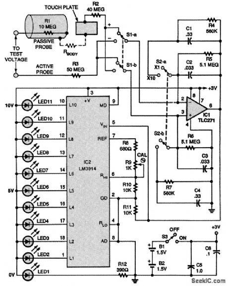
This probe for low voltages only (<100 V) uses the body to complete the dc circuit in a novel way. The schematic for the dc voltmeter is shown. Power for the circuit is provided by two 1.5-V N-type cells, B1 and B2, which are wired in series. For the circuit to work, it must be completed or closed. That is accomplished when the passive probe is held in one hand and the active probe is held in the other and the points of the two probes are placed across two points in a circuit under test. The resistor labeled Rbody is simply the resistance of the user's body. For Rbody to be swamped out, or kept from interfering with the reading, extremely high input-circuit impedances are used in the circuit. All of the people tested by the author for this project indicated a body resistance from hand to hand in the range of 200,000 to 500,000 Ω. Therefore, an input impedance of 50 MΩ, resistor R3, was added. That also provided an adequate safety isolation feature. The reduction of RFI and 60-Hz pickup is accomplished by the use of a symmetrical difference amplifier (IC1) at the input; the inherent common-mode rejection takes care of most the ac-related problems. The amplifier used for IC1 is a TLC271 CMOS op amp. Switch S1 is used to select polarity. Note that 50 MΩ of resistance are present at both of IC1's differential inputs (R3 at one input and the combined series resistance of R1 and R2 at the other). The user is placed in series with the 100-MΩ loop containing a 10-MΩ resistor (R1) as the protective device in the passive-probe section. Capacitors C1 to C4 provide additional filtering of residual ac noise and allow IC2, an LM3914 bar-graph display driver, to step up sequentially. Switch S2 selects between two selectable input ranges: XI, where each step equals 1 V, and X10, where each step equals 10 V. The display is made up of LED1 to LED11; LED2 through LED11 indicate the individual steps. LED1, the 0-V indicator, is also the power-on indicator. (View)
View full Circuit Diagram | Comments | Reading(1309)
HALF_SQUARE_MAGNETIC_MULTIPLIER
Published:2009/7/17 1:55:00 Author:Jessie

Can be used as squaring function generator, quarter-wave multiplier, or two multipliers. Only one operational amplifier is required.-T. Miura and C. Hirano, Reliable Magnetic Amplifier Improves Multiplier, Electronics, 35:26, p 76-79.
(View)
View full Circuit Diagram | Comments | Reading(738)
12_V_AT_10_A
Published:2009/7/17 1:55:00 Author:Jessie

Permits AC operation of 12-V FM transceiver. Article tells how to rewind 12-V TV power transformer rated above 120 W with No.12 enamel to get required 18-V secondary. If original winding has 2 turns per volt, new secondary will need 36 turns. Q1 is HEP233, HEP237, or similar transistor rated 10 A or higher, with heatsink, U1 is 25-A 100-PlV bridge rectifier, and U2 is National LM340K-12 regulator. CR1 can be any rectifier rated at least 3 A at 35 V. - L. McCoy, The Ugly Duckling, QST, Nov.1976, p 29-31. (View)
View full Circuit Diagram | Comments | Reading(1004)
VOLTAGE_TO_FREQUENCY_CONVERTER_I
Published:2009/7/11 5:14:00 Author:May
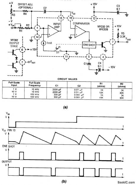
Using a Burr-Brown VFC 32 IC, this voltage-to-frequency convener uses few components. The circuit values are shown in the figure.This charge-balanced V/F converter uses a VFC32 or a VFC320 IC. The positive charge from the 1-mA balances the negative charge from the input. V/F converter waveforms are shown in Fig. 100-1(b). (View)
View full Circuit Diagram | Comments | Reading(802)
REFLEX_KLYSTRON_FREQUENCY_AND_VOLT_AGE_CONTROL
Published:2009/7/17 1:53:00 Author:Jessie
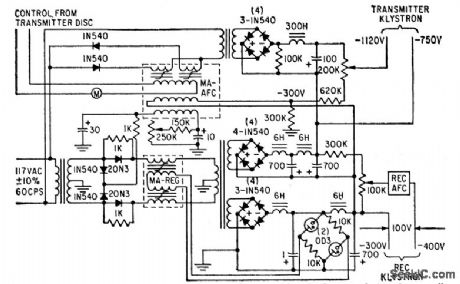
Consists of main regulation magnetic amplifier MA-REG for reflect or VA-222 power klystron in 6,000-Mc microwave link, and secondary magamp MA-AFC that provides further regulation for repeller voltage.-J. Markus, Handbook of Electronic Control Circuits, McGraw-Hill, N.Y., 1959, p 110.
(View)
View full Circuit Diagram | Comments | Reading(2539)
ADJUSTABLE_D_C_LEVEL_SHIFTER
Published:2009/7/17 1:53:00 Author:Jessie

Shills d-c level of signal accurately and continuously without affecting gain, from +4 V to +z V d-c center-voltage output. Input ac signal varies 2 v about +4 v d-c. Other offset voltages can also be obtained.-H Anway Continuously Adjustable DC Level Shifter, EEE, 12:10, p 59. (View)
View full Circuit Diagram | Comments | Reading(1005)
SYNCHRONOUS_SWITCHING_BOOSTS_VOLT_AGE_GAIN
Published:2009/7/17 1:49:00 Author:Jessie

Synchronously switched biased diodes insert impedance in control circuit during power half-cycle. During reset half-cycle bias rectifiers conduct and signal is applied directly across control windings to increase gain by factor of four.-J. Markus, Handbook of Electronic Control Circuits, McGraw.Hill, N.Y., 1959, p 115. (View)
View full Circuit Diagram | Comments | Reading(543)
LOGIC_PROBE_1
Published:2009/7/17 1:48:00 Author:Jessie

The circuit uses a 4N35 optocoupler (IC1) and a C9013G transistor (Q1). A positive pulse at the base of Q1 turns on the transistor. The 10,000-Ω resistor (R2) limits the incoming pulse so as not to feed too much current to the base of Q1, preventing the transistor from being damaged. With the base of Q1 at a positive potential, electron current flows from the emitter to the collector junction. The incoming pulse also pulls pin 6 high, lighting up LED1 by allowing current to flow between pins 4 and 5. The 330-Ω resistor (R3) provides current limiting for pin 6, although R4 is the current limiter for pin 4. While testing a digital circuit, if the LED lights, that portion of the circuit is in a high state; if the LED remains off, a low is present. The circuit can be placed inside a small enclosure if its connections are made as short as possible. (View)
View full Circuit Diagram | Comments | Reading(6186)
PULSE_STRETCHER
Published:2009/7/17 1:48:00 Author:Jessie
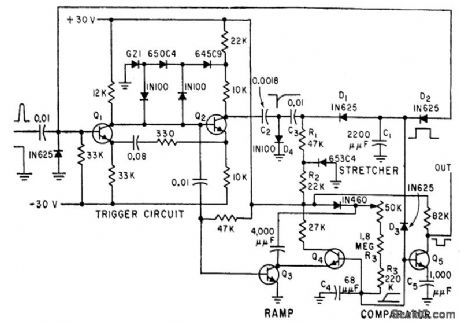
Used where low-amplitude pulses must be converted to time in. formation. Output is used to control oscillator.-D. N. Carson and S. K. Dhawan, Data Conversion Circuits for Earth Satellite Telemetry, Electronics, 33:3, p 82-84. (View)
View full Circuit Diagram | Comments | Reading(0)
OPAMP_TESTER
Published:2009/7/11 5:12:00 Author:May

Developed for quick testing of 741 and 301 opamps. For good opamp, LEDs flash alternately with 1-s period. No flashing and no illumination indicate opamp output fault. If one of LEDs glows continuously, one of inputs is faulty. Asymmetrical blinking indicates leakage in opamp.-Circuits, 73 Maga-zine, March 1977, p 152. (View)
View full Circuit Diagram | Comments | Reading(2485)
3_50WPM_KEYER
Published:2009/7/11 5:12:00 Author:May

Uses NE555V 1 as switchable dot generator providing accurate 1 : 1 ratio.SN7473 U2 forms variable dash circuit. NE555V sidetone generator U4 has tone range of about three octaves and easily drives 3-W 4-ohm loudspeaker through small transistor-radio transformer TR. NE555V US acts with U4 to provide two-tone oscillator for SSB tuning. Output section Q1-Q2 easily handles keying bias of -26V at 5 mA.-H. Seeger, Micro-TO Keyer Mods,Ham Radio,July 1976,p 68-59. (View)
View full Circuit Diagram | Comments | Reading(1260)
LOW_CURRENT_VOLTAGE_TRIPLER
Published:2009/7/11 5:08:00 Author:May
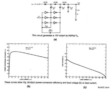
Using a 74HC14 operating at 350 kHz,this voltage tripler delivers approximately 12 V from a 5-V Supply. (View)
View full Circuit Diagram | Comments | Reading(588)
AMPLITUDE_COMPARATOR
Published:2009/7/11 5:07:00 Author:May

Uses minimum-hysteresis Schmitt trigger (30 my hysteresis) to compare voltage at input B with that at input A Can also be used as variable Schmitt trigger in which input B determines trigger voltage.-M. A. Smither and W. E. Zrubek, Variable Schmitt, Amplitude Comparator, EEE, 14:7, p106. (View)
View full Circuit Diagram | Comments | Reading(1136)
BINAURAL_SYNTHESIZER_FOR_CW
Published:2009/7/11 5:06:00 Author:May

Provides two channels for feeding stereo phones or two loudspeakers. When interference occurs a few hundred hertz from desired frequency, receiver is tuned so desired signal appears to be midway between loudspeakers, leaving interfering signals at right or left. Left or low channel has low-pass active filter and right or high channel has high-pass filter, with crossover at 750 Hz. Synthesizer is designed for low-impedance drive, as from loudspeaker output of receiver. Resistors in output channels prevent oscillation when 8-ohm phones or loudspeakers are directly connected to outputs. Opamps will drive 2000-ohm phones with ample volume and give moderate volume levels with 8-ohm loads.-D. E. Hildreth, Synthesizer for Binaural CW Reception, Ham Radio, Nov. 1975, p 46-48 (View)
View full Circuit Diagram | Comments | Reading(1368)
CW_SIDETONE
Published:2009/7/11 5:05:00 Author:May
Audio sidetone oscillator serves for monitoring CW keying. Changes in transmitter operating frequency do not affect sidetone circuit. Hartley AF oscillator Q2 is turned on by diode rectifier and DC amplifier Q1.Antenna coupling shown is adequate from 160 through 10 meters. For VHF use on 6 and 2 meters, small tuned circuit and pickup antenna are usually required to get enough RF input for monitor. Audio pitch is adjusted by changing value of C1.-J. Fisk, Circuits and Techniques, Ham Radio, June 1976, p 48-52. (View)
View full Circuit Diagram | Comments | Reading(2745)
2000_V_LOW_CURRENT_POWER_SUPPLY
Published:2009/7/11 5:05:00 Author:May

In this circuit Q1, Q2, R1, and C1 form a multivibrator. The square wave that results from the oscillation of this circuit (20 to 30 Vpp) is stepped up by T1 (an audio transformer of the type used in radios or small TVs). An 8- to 1,200-Ω impedance ratio equates to a turn ratio of 12:1. The ac from the secondary of T1 is applied to the multiplier circuit (D1 to D8 and C2 to C9). NE1/R2 are used as an operating indicator. The circuit will supply about 2,000 V. C2 to C9 should have a 400-V or higher voltage rating. (View)
View full Circuit Diagram | Comments | Reading(684)
PASSIVE_CW_FILTER
Published:2009/7/11 5:05:00 Author:May

Uses inexpensive 88-mH toroids to give very sharp 35-Hz bandwidth at 3 dB down. Filter has high insertion loss. Keyed waveshape has slow rise and fall, so CW signals have pronounced ringing that may be objec-tionable.-A. F. Stahler, An Experimental Com-parison of CW Audio Filters, 73 Magazine, July 1973, p 65-70. (View)
View full Circuit Diagram | Comments | Reading(1473)
BILATERAL_TRANSISTOR_COMPARATOR
Published:2009/7/11 5:04:00 Author:May

Used as voltage comparator by connecting one input to some reference level and allowing sec ond input to vary. Can also serve as digital comparator in digital computer, to ascertain when two numbers become equal. Output drops to zero when numbers in digital form are equal.-Comparator Uses Bilateral Tran-sistor, Electronic Circuit Design Handbook, Mactier Pub. Corp, N.Y. p91. (View)
View full Circuit Diagram | Comments | Reading(916)
| Pages:770/2234 At 20761762763764765766767768769770771772773774775776777778779780Under 20 |
Circuit Categories
power supply circuit
Amplifier Circuit
Basic Circuit
LED and Light Circuit
Sensor Circuit
Signal Processing
Electrical Equipment Circuit
Control Circuit
Remote Control Circuit
A/D-D/A Converter Circuit
Audio Circuit
Measuring and Test Circuit
Communication Circuit
Computer-Related Circuit
555 Circuit
Automotive Circuit
Repairing Circuit