
Circuit Diagram
Index 772
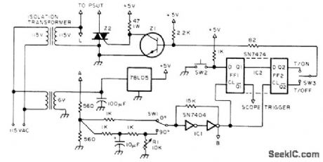
QUAD_OPAMP_TESTER
Published:2009/7/11 4:39:00 Author:May

Interface circuit shown permits use of single-opamp tester for testing quads without major modification of tester's original function. Interface operates on power available from tester, which can be Teledyne/Philbrick 5102 or current Tektronix or ESI testers. CM0S input transmission gates IC1 and IC2, supply input signals to sections of device under test (DUT). Gate control signals are supplied by section selector S1; switch can be automated by using two-line BCD selection, Same switch also activates reed relay that cona nects respective amplifier section to load and output monitoring circuits of tester. LEDs indicate section under test. Interface can be used with LM124, CA124, and MC3503 series of quad opamps.-A. C. Svoboda, Use a Single Op-Amp TesterforQuads, EDN Magazine, March 5, 1975, p76. (View)
View full Circuit Diagram | Comments | Reading(1402)
DYNAMIC_LOAD
Published:2009/7/11 4:37:00 Author:May
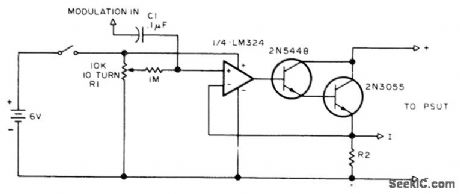
R1 sets load current drawn from power supply under test to desired value, after R2 is chosen to give about 1-V output at maximum load currentto be drawn from power supply under test (PSUT). Modulation input to C1 is obtained from external pulse generator, and selves to make load current increase and decrease over small range.-R. Tenny, Power Supply Testing, 73 Magazine, July 1976, p 112.114 and116-117. (View)
View full Circuit Diagram | Comments | Reading(784)
STABILIZED_LOW_FREQUENCY_OSCILLATOR
Published:2009/7/11 4:36:00 Author:May

Transistors Q1 and Q4 compare charging voltages of mvbr timing capacitors C1 and C2 to fixed reference voltage.When a capacitor voltage is greater than reference.its comparator switches its bistablw mvbr to opposite state,so capacitor is discharged by dump transistor.Arrangement makes output frequency essentially independent of temperqture from-25℃ to+75℃.for frequency range of 0.01 to 100,000 cps,-J.D.Long.Novel Differential Amplifier Stabilizes Multivibrator,Electronics,35:24,p53-54 (View)
View full Circuit Diagram | Comments | Reading(728)
CW_STEREO_FILTER
Published:2009/7/11 4:35:00 Author:May

Developed to enhance ability to read CW despite heavy contest traffic or other QRM. Two high-Q filters, one at each end of 400-Hz CW filter in receiver, create separate audio channels to give effect of stereo.Transistors at outputs of channels provide extra current gain for driving low-impedance stereo headphones. CW signal at 800 Hz then appears to comefrom left, 1200-Hz signal from right, and in between frequencies at various azimuth angles. Illusion of direction makes it easier for operator to concentrate on desired signal in presonce of others having slightly different frequencies. L1 and C1 form filter for 1200-Hz channel, while L2 and C2 form 800-Hz filter for other channel.-R. L. Anderson, Stereo-a New Type of CW Filter, 73 Magazine, March 1976, p 48-50. (View)
View full Circuit Diagram | Comments | Reading(854)
VOLTAGE_MULTIPLIER
Published:2009/7/11 4:35:00 Author:May

Figure 99-l(a)'s circuit exhibits a high-output impedance as a result of the small effective capacitance of the series-connected capacitors, and it exhibits considerable voltage loss due to all of the diode drops. Further, this circuit requires 2n diodes and 2n capacitors to produce a dc output voltage approximately n times the rail voltage.Figure 99-1(b)'s circuit multiplies more effectively using fewer diodes and capacitors. The parallel arrangement of the capacitors lets you use smaller capacitors than those required in Fig. 99-1(a). Alternatively, when using the same capacitor values of Fig. 99-1(a), the output impedance will be lower.Whereas the clock source directly drives only one of the two strings of capacitors in Fig. 99-1(a), Fig. 99-1(b)'s clock drives both strings with opposite phases. This drive scheme doubles the voltage per stage of two diodes. A final diode is necessary to pick off the dc output voltage because both strings of capacitors now carry the p-p ac input-voltage waveform. The ICL7667 dual-FET driver accepts a TTL drive swing and provides a low-impedance push-pull drive to the diode string. This low impedance is particularly helpful when using a long string to raise output voltage to more than 100 V, starting from a low rail voltage. (View)
View full Circuit Diagram | Comments | Reading(1069)
WEAK_SIGNAL_DECODER
Published:2009/7/11 4:35:00 Author:May

Combination of narrow-bandpass 800-Hz active filter and phase-locked loop of tone decoder permits copying very weak signals in Morse code. LED provides visual indication supplementing conventional output for headphones or loudspeaker.-Circuits, 73 Magazine, July 1977, p 35. (View)
View full Circuit Diagram | Comments | Reading(691)
DIFFERENTIAL_VOLTAGE_COMPARATOR
Published:2009/7/11 4:34:00 Author:May
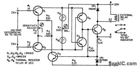
If the two input signals are within preset differential voltage relay is not actuated and GO indicator comes on.When the two signal differ too much,relay is actuated and NO-GO indication is provided.Used in commparing telemetered data received from satellite vehicle.-P.A.Walter,Differential Voltage Comparator.EEE.10:8,p24-25 (View)
View full Circuit Diagram | Comments | Reading(616)
CW_IDENTIFIER
Published:2009/7/11 4:34:00 Author:May
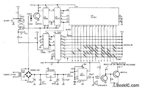
Circuit automatically gener ates call Ietters for FCC-required code identification for FM repeaters and RTTY, when started by pushbutton or by pulse from other equip ment. Audio output can be fed to loudspeaker as monitor or used to modulate FM repeater.Circuit shown is programmed for DE K4EEU by installing diodes at locations where tone is wanted on matrix. Article gives construction and programming details.-B. Kelley, A Super Cheapo CW IDer, 73 Magazine, Dec. 1976, p 46-48. (View)
View full Circuit Diagram | Comments | Reading(2016)
VCO
Published:2009/7/11 4:31:00 Author:May


Q1. an FET. is used as a variable resistance to control frequency of oscillator. (View)
View full Circuit Diagram | Comments | Reading(0)
CMOS_KEYER_3
Published:2009/7/11 4:30:00 Author:May

Uses two CD4001AE quad two-input N0R gates. Q1A-Q1B form time-base MVBR, and Q1C-Q1D form dash flip-flop. Three of remaining gates synthesize three-input NOB gate for dash control. Q2D controls time-base MVBR and provides keyer output. Speed is adjustable from below 10 to over 70 WPM with R3.-C. J. Bader, Improved CW Transceiver for 40 and 80 Ham Radio, July 1977, p 18-22. (View)
View full Circuit Diagram | Comments | Reading(725)
AUTOMATIC_HI_ON_HORN
Published:2009/7/11 4:29:00 Author:May
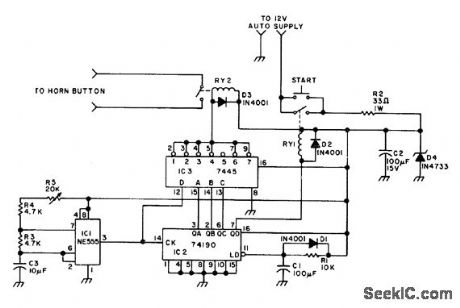
Pressing start button of circuit momentarily makes it send letters H1 in Morse code on automobile horn, as friendly signal to another ham on road. Uses NE555 timer as oscillator, acting with counter 102, decoder IC3, power-supply latch, and regulator. Space betweqn four dots of H and two dots of I is achieved by not using pin 5 of decoder. RY1 should pull in at 5 V and 16 mA maximum,while RY2 should pull in at 5V and 80 mA maximum and have contacts for switching 0.5-A inductive load of horn.-J. F. Reid, Sending HI, 73 Magazine, May 1977, p 90. (View)
View full Circuit Diagram | Comments | Reading(1004)
VARACTORLESS_VCO
Published:2009/7/11 4:28:00 Author:May

The varactorless VCO utilizes a modifted Clapp-oscillator conftguration, together with some data on the type of transistor, circuit values, and operating frequencies. (View)
View full Circuit Diagram | Comments | Reading(822)
OUASI_BREAK_IN
Published:2009/7/11 4:28:00 Author:May
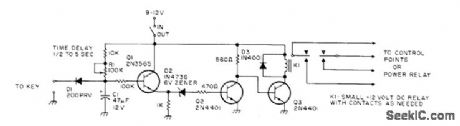
Amateur station stays in receive mode until operator starts to send code. Tapping on key makes transmitter switch into transmit mode and stay there after last character is sent, for delay of several seconds (determined by R1) before transmitter is deenergized, Developed for use with cathode-keyed transmitters,-F,E,Hinkle,Jr,KOX for CW 73 Magazine, Feb 1975,p 129-130. (View)
View full Circuit Diagram | Comments | Reading(556)
TUNNEL_DIODE_VOLITAGE_COMPARATOR
Published:2009/7/11 4:27:00 Author:May

When incoming signal exceeds predetermined leverl,pulse with predetermined amplitude appears at output.-T.Kolima and M.Watanabe,When You're Second,You Try Harder,Electronics,38:25,p81-89 (View)
View full Circuit Diagram | Comments | Reading(563)
TTL_GO_NO_GO_TESTER
Published:2009/7/11 4:26:00 Author:May

Test panel provides fast static test of surplus 7400 series TTL ICs. Each contact of 16-pin DIP socket has lead that can be plugged into array of seven othersockets carrying various supply voltages, loads, etc. Switches provide pulses of input current for toggling or clocking, counting, and resetting. Leads also serve for cross-coupling gates in IC to make flip-flop and forsetting up other simple circuits. Input voltage control allows plotting of transfer functions and study of circuit operation under different signal-level conditions. Extemal test meter can be connected when necessary. HI and LO indicators are LEDs that show level of terminal connected to output socket. Transistors are general-purpose NPN such as 2N2926. U1 is SN7404 hex inverter, and U2 is SN7400 quad two-input NAND gate. Tester is not suitable for complementary MOS devices requiring protection from static charges. Article gives detailed instructions for testing each type of TTL device.-J. S. Worthington, A Simple TTL Test Panel, QST, Dec. 1976, p 25-27. (View)
View full Circuit Diagram | Comments | Reading(1626)
WIDE_RANGE_VCO
Published:2009/7/11 4:24:00 Author:May

This circuit covers 0 to 1.4 kHz.C1 can be changed to cover other ranges,as desired. (View)
View full Circuit Diagram | Comments | Reading(1065)
POWER_DIODE_TESTER
Published:2009/7/11 4:24:00 Author:May

Provides revelse-voltage test of individual sections of rectifier stackat 1000 VDC,With test leads E1 and E2 clippedacross diode section under test,Variac setting is increased from 0 until C1 is charged to 1000 V as indicated by voltmeter. If diode or capacitor in section under test is defective, meter will read Iow because of extra voltage loss across R1 Initial setup is made with good diode section, Open S1 before changing diode because voltage is lethal.-R. K. Dye, Testing Dye-Odes, QST, Feb. 1976, p 44. (View)
View full Circuit Diagram | Comments | Reading(976)
AF_SIGNALTRACER
Published:2009/7/11 4:23:00 Author:May
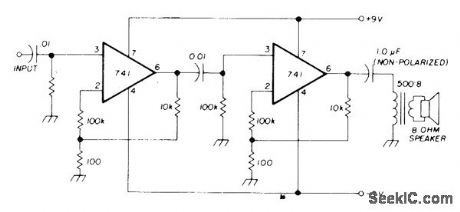
High-gain audio amplifier with loudspeaker output serves for troubleshooting AF stages. With normal input to amplifier under test, presence of AF signal is tested in each stage in turn. If AF signal appears at input of stage but not at output, that stage has a defect. Signal source may also be signal injector having broadband output from audio through VHF.-M. James, Basic Troubleshooting, Ham Fladio, Jan. 1976, p 54-57. (View)
View full Circuit Diagram | Comments | Reading(551)
PORTABLE_TRANSISTOR_TESTER
Published:2009/7/11 4:22:00 Author:May

Go/no-go tester shows relative condition of NPN and PNP transistors, junction FETs, and dual-gate MOSFETs. Not suitable for checking audio or highpower RFtransistors. Crystal for upper range of HFspectrum is permanently wired; any HF crys-tal cut for fundamental-mode operation can be used. Rectified RF from oscillator is monitored on M1. S1 selects negative ground for testing N-ehdnnel FETs and NPN bipolars and provides positive ground for P-ehannel and PNP devices. If device is open, shomed, or extremely Ieaky, circuit wiII not oscillate and meter will not deflect. The higher the meter reading, the higher the gain of transistor at operating frequency. When testing MOSFETs that are not gate-protected, keep transistor Ieads shorted until device is in socket and replace short before re moving device. Diodes are 1N34A or equivalent.-D. DeMaw and C. Greene, A Pair of Handy Testers, QST, May 1973, p 24-27. (View)
View full Circuit Diagram | Comments | Reading(1253)
VIBRATION_DETECTOR
Published:2009/7/17 3:01:00 Author:Jessie

Low-frequency boost compensates for characteristics of velocity-type vibration detector for turbines. Detector voltage is proportional to both displacement and frequency, so integrating action by capacitance feedback around high-gain amplifier stage makes output proportional to displacement only.-H. A. Harriman and W. M.Trenholm, Vibration Measurements with Peak-Reading Circuit, Electronics, 35:20,p 57-59. (View)
View full Circuit Diagram | Comments | Reading(1719)
| Pages:772/2234 At 20761762763764765766767768769770771772773774775776777778779780Under 20 |
Circuit Categories
power supply circuit
Amplifier Circuit
Basic Circuit
LED and Light Circuit
Sensor Circuit
Signal Processing
Electrical Equipment Circuit
Control Circuit
Remote Control Circuit
A/D-D/A Converter Circuit
Audio Circuit
Measuring and Test Circuit
Communication Circuit
Computer-Related Circuit
555 Circuit
Automotive Circuit
Repairing Circuit