
Circuit Diagram
Index 762
BUFFER_MEMORY_SENSE_AMPLlFIER
Published:2009/7/12 21:13:00 Author:May
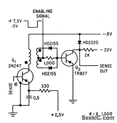
Uses coincident-current technique. Full-wave rectifier is required at secondary of transformer because sense output can be of either polarity. Enabling signal turns on sense amplifier, to permit discrimination between memory core outputs during unload and load cycles.-D.Haagens, Compact Memories Have Flexible Capacities, Electronics, 32:40, p50-53. (View)
View full Circuit Diagram | Comments | Reading(626)
15_min_DELAY
Published:2009/7/12 21:13:00 Author:May
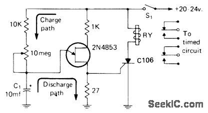
When S1 is closed, C1 begins charging, After delay determined by setting of 10-megohm pot, UJT conducts and makes C1 discharge through 27-ohm resistor, triggering SCR C106 and energizing relay. 0pen S1 to reset circuit.-I, Math, Math's Notes, C0, April 1974, p 64-65 and 91-92.
(View)
View full Circuit Diagram | Comments | Reading(938)
S_R_FLIP_FLOP
Published:2009/7/12 21:13:00 Author:May
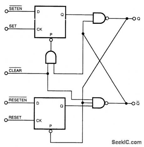
This circuit combines the characteristics of an asynchronous S/R flip-flop and an edge-triggered JK flip-flop. It changes state on the leading edges of its inputs, and ignores the levels at all other times.In operation, outputs of both D flip-flops are normally high, going low for brief periods after seeing an edge at their respective clock inputs. (View)
View full Circuit Diagram | Comments | Reading(1164)
SCANNING_KEYBOARD_WITH_MEMORY
Published:2009/7/12 21:12:00 Author:May
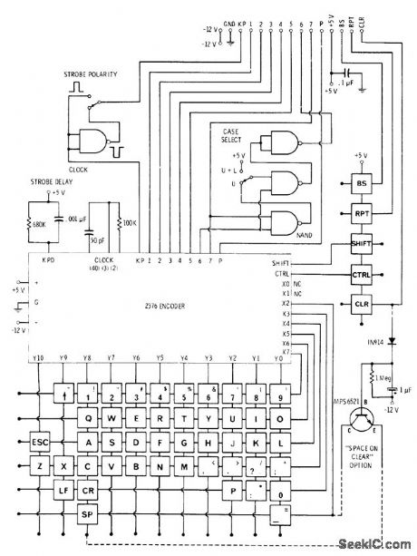
Standard keyboard is updated to 53 keys as required for character feed in microprocessorbased TV typewriter system. Features include two-key rollover, along with choices of letter case, strobe polarity, clear key, and repeat key.Space output is produced automatically during clear.-D. Lancaster, TV Typewriter Cookbook, Howard W. Sams, Indianapolis, IN, 1976.p 150-151. (View)
View full Circuit Diagram | Comments | Reading(772)
CAPACITOR_ALLOWS_HIGHER_SLEW_RATES
Published:2009/7/12 21:11:00 Author:May
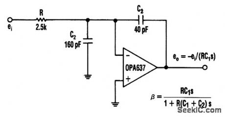
In this circuit, a Burr-Brown op amp supplies a slew rate of 135 V/μs. The addition of C2 charges the high-frequency feedback factor to less than unity, and allows higher slew-rate amplifiers to be compensated for greater-than-unity gain. (View)
View full Circuit Diagram | Comments | Reading(721)
FLASHING_LED_EGG_TIMER
Published:2009/7/12 21:10:00 Author:May
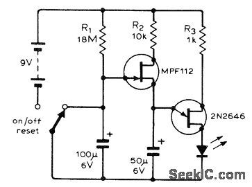
UJT oscillator controlled by FET timer makes LED flash after time delay determined by value of R1. When 100μF capacitor charges to about 1 V after switch is turned on, MPF112 FET switches on and forms part of charging circuit for 2N2646 UJT oscillator which then pulses LED at about 200 mA peak. Although developed as inexpensive egg timer, circuit has many other applications.-J. Jeffrey, Simple FlashingL.E.D. Timer, Wireless World, Oct. 1974, p 381. (View)
View full Circuit Diagram | Comments | Reading(2735)
PRESEITABLE_ANALOG_TIMER
Published:2009/7/12 21:09:00 Author:May
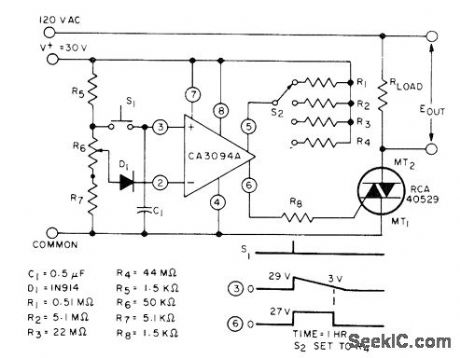
Switch S2 gives choice of four delay intervals between closing of S1 and triggering of triac by RCA CA3094A programmable power switch and amplifier,Pot R6 is required for initial time set. - Linear Integrated Circuns and MOS/FET's, RCA Solid State Division、Somerville,NJ,1977, p 192-196.
(View)
View full Circuit Diagram | Comments | Reading(799)
FULL_WAVE_RECTIFIER_TO_10_MHz
Published:2009/7/12 21:09:00 Author:May

Using two CA3450 op amps and a CA3227 transistor array, this circuit will accurately full-wave rectify signals to 10 MHz. Two of the CA3227 transistors drive the output, two are in the feedback circuits. Two transistors serve as clamping diodes, limit the negative-going signals of each amplifier, and keep both amplifiers active during the end cycle. The maximum output is determined by the slew rate of 300 V/μs at highest frequencies. This output equals 300 V/ms÷6πV peak. (View)
View full Circuit Diagram | Comments | Reading(756)
GATE_AND_MIXER_FOR_10_NSEC_PULSES
Published:2009/7/12 21:08:00 Author:May
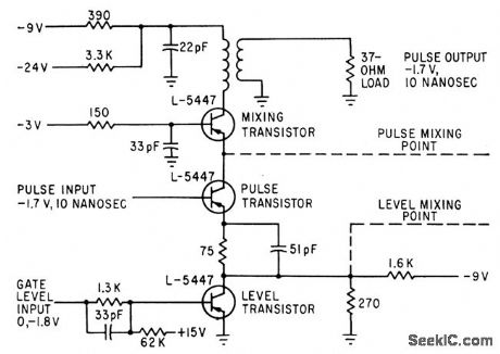


Used in 50-megapulse computer.Propagation delay time of circuit is only 4.5 nsec.Transistors may also be 2N769 or 2N976-K,H.Konkle and J. E. Laynor, Key to Faster Computers:Ten-Nanosecond Amplifer.Electronics,35:50,p39-41. (View)
View full Circuit Diagram | Comments | Reading(579)
HEX_ENCODER_FOR_KEYBOARD
Published:2009/7/12 21:07:00 Author:May
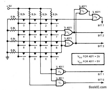
Standard 16-button keyboard is used with CMOS packages to provide hex output bits. Pressing one button increases voltage on its horizontal line from 0 to 2.2 V. If button is in other than first row, OR gate U3 or U4 is activated and either bit 2 or 3 changes from LOW to HIGH. Simultaneously, voltage of vertical column of button decreases from 5 V to 2.2 V. If button is in other than first column, NAND gate U1 or U2 is activated and either bit 0 or 1 changes from LOW to HIGH. OR gates U5 and U6 provide button-pressed signal by changing bit 7 from LOW to HIGH upon activation of any button.-W. H. Hailey, CMOS Logic Implements Keyboard Encoder, EDN Magazine, Aug. 5, 1978, p 54 and 56. (View)
View full Circuit Diagram | Comments | Reading(1751)
10min_ID_TIMER
Published:2009/7/12 21:07:00 Author:May
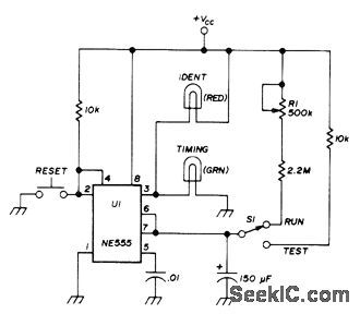
Red pilot lamp comes on at end of timing period, adjustable with R1 from 7 to 11 min, as reminder for amateur radio operatorto makestation identification required by FCC every 10 minutes. Green lamp indicates that timer is on and timing. Lamps should draw no more than 100 mA, to avoid overloading NE555 timer. Any 9-12 VDC supply can be used.-D. Backys, ldentification Timer, Ham Radlio, Nov. 1974, p 60-61. (View)
View full Circuit Diagram | Comments | Reading(811)
FULL_ADDER
Published:2009/7/12 21:06:00 Author:May
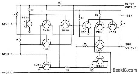
Made by joining two half-adders. Push-pull inverting amplifiers serve as switches to provide completely automatic operation. Carry from full adder can derive from either half-section but never both. No inhibitor signal is required to suppress un wanted sum signal,-F. B. Maynard, Half-Adders Drive Simuhcmeous Computer, Electronics, 31:29, p80-82. (View)
View full Circuit Diagram | Comments | Reading(2218)
RADIO_TURNOFF
Published:2009/7/12 21:05:00 Author:May
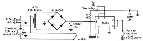
Time-delay control R2 canbe set to turn off radio,TV or other applianceat any desired interval between about 3 and 60 min after start buttonis pushed,ldealfol those who fall asleep to music. K1 is 12-V relay drawing 200 mA ot less.-P. Walton, An Electronic Timer for Less than $5.00, CQ, Aug. 1973, p 42 and 82. (View)
View full Circuit Diagram | Comments | Reading(543)
ULTRA_SIMPLE_RS232_TESTER
Published:2009/7/12 21:05:00 Author:May
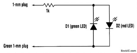
The tester consists of no more than a two-color LED (or a red and a green LED connected in anti-parallel) in series with a 1-kΩ resistor. The free ends of the resistor and the LEDs should preferably be terminated in 1-mm plugs. One of the free ends should be covered in green sleeving, or use a green 1-mm plug. This is touched on pin 7 (signal ground) of the connector under test. The other end is touched on each pin to be tested, in turn. The LED (or LED pair) is connected so that a positive voltage emits a red glow and a negative voltage causes a green glow. Sometimes, an RS232 input will be found that has an internally connected pull-up to drive a particular default RS232 level when unconnected. Although this will cause the tester to glow as if the pin were an output, it will do so with markedly less brightness. Bearing this in mind, the tester can be used to diagnose most RS232 problems at the electrical level. (View)
View full Circuit Diagram | Comments | Reading(3259)
COMPUTER_SERIAL_PORT_RELAY_CONTROLLER
Published:2009/7/12 21:03:00 Author:May

Decoding RS-232 signais is a job for a microcontroller (single-chip computer). Fortunately, you don't have to program the microcontroller yourself; you can get a PIC 16C54A microcontroller already programmed for exactly this job from Stone Mountain Instruments. Shown is the circuit and the BASIC program to demonstrate how it works. Each SMI101B has eight logic-level outputs.Further, you can connect up to seven SMI101Bs to a single serial port. The three N pins give each SMI101B a distinctive identifying number, from 0 to 6. If all three are grounded, the identifier is 0; if N1 is connected to +5 V, the identifier is 1, etc. At power-up, all the data outputs are off (logic 0). To turn an output on, send a command of the form xNy, where x is the identifier of the SMI101B and y indicates which data output you want to switch, To turn the outputs back off, use an F in place of an N (e.g., OF3). All communication is done with 8 data bits and no parity bits. The baud rate is 9600 baud with a 4-MHz crystal, or 1200 baud with a 500-kHz ceramic resonator. As shown in the diagram, each relay requires a transistor to drive it, along with a resistor and a protective diode. To cut down the total number of components, you can use a relay driver chip, such as the Allegro UDN2987, which contains everything necessary to drive eight small relays from logic-level signals. (View)
View full Circuit Diagram | Comments | Reading(2157)
HARMONIC_GENERATOR
Published:2009/7/12 21:02:00 Author:May
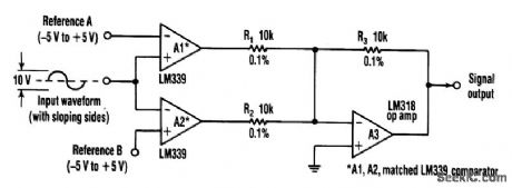
This circuit can extract harmonics from various waveforms. With a sloped input waveform, the comparator produces a pulse width that is proportional to a reference plus input amplitude. As the pulse width changes, the harmonics spectrum changes. Combining the two comparator outputs eliminates some harmonics, depending on the duty cycle. Adjusting the references can create virtually any harmonic.A1 and A2 should be matched, R1 and R2 should be equal to 0.1%, and A3 should have good common-mode rejection and high slew rate. (View)
View full Circuit Diagram | Comments | Reading(0)
SIGNAL_CONDITIONER
Published:2009/7/12 21:00:00 Author:May
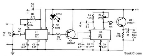
This circuit takes audio from a receiver that might have a weak CW or tone signal and uses a PLL (U1) to recover the weak signal. U1 produces a low on receipt of a tone or note of frequency, determined by R1, R7, and C2. The output of U1 (pin 8) goes low, keys tone generator U2, and produces a new tone. The circuit is useful in cleaning up CW reception in static. noise. etc. (View)
View full Circuit Diagram | Comments | Reading(682)
ISOLATED_RS232_INTERFACE
Published:2009/7/12 21:00:00 Author:May

Electrical isolation of 1500 V or higher is possible with this cost-effective RS232 interface. It is ideal for various data-communication designs, including medical instrumentation and devices within harsh electrical environments. The interface uses the host's TXD (transmit data), RXD (receive data), DTR (data terminal ready), and RTS (request to send) lines to provide power.For fully duplexed operation, the host's communications port should be set up so that its RTS is off (at negative voltage). Halfduplex operation can use the host's TXD negative voltage, available through D6, to run the circuitry. Sending a low bit (space state) to the host is just the opposite. This time, the required positive voltage is supplied from the host via diodes D2 and D3, and is routed through Q1 and D1 to DB9-2. (View)
View full Circuit Diagram | Comments | Reading(1633)
PRINTER_PORT_D_A_CONVERTER
Published:2009/7/12 20:58:00 Author:May
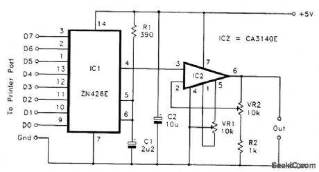
Where eight latching outputs are available, the Ferranti 2N426E probably represents the simplest means of providing an analog output. The figure shows the circuit diagram for a PC analog output port based on this chip. The full-scale output voltage is equal to the reference voltage fed to pin 5. This terminal can be fed from an external reference voltage of up to 3 V, but, in most cases, the built-in 2.55-V reference is perfectly adequate. The output voltage from IC1 (in volts) is equal to the value written to the printer port multiplied by 0.001. In most practical applications, this output-voltage range will have to be modified using an amplifier or an attenuator. In virtually all cases it will be a small amount of amplification that is required. This is the purpose of IC2, which also provides output buffering. The noninverting-mode amplifier IC2 can have its closed-loop voltage gain varied from unity to about 11 times by means of preset VR2.The maxinum output voltage of IC2 is about 2 V less than its supply potential (about 3 V) if it is powered from a 5-V supply. Therefore, maximum output voltages of more than 3 V require IC2 to be powered from a higher supply potential of up to about 30 V. This means using a separate supply for IC2 because the converter circuit must be powered from a 5-V supply. If preset VR1 is included, the best way to find the correct setting is to first write a low value to the port and adjust VR1 for the correct output voltage. Then write a high value to the port and adjust VR2 for the appropriate output voltage. Repeat this process a few times until no further adjustment is needed. If VE1 is omitted, write a value of 255 to the port and then adjust VR2 for the required maximum output voltage. Reasonable accuracy should then be obtained over the full range of output voltages.Using GW BASIC, it is just a matter of writing the values to the appropriate address using the OUT command. For example, OUT &H378,123 would write a value of 123 to a digital-to-analog converter connected to printer port LPT1. (View)
View full Circuit Diagram | Comments | Reading(810)
TIME_SHARED_TROUBLESHOOTER_SCOPE
Published:2009/7/12 20:58:00 Author:May

Oscilloscope modifications shown permit computer to control cro display for diagnosing trouble in faulty section of time-sharing comcomputer.-J. T. Quatse, Time-Shored Trouble-shooter Repairs Computers On-Line.Electronics,39:2,p97-101. (View)
View full Circuit Diagram | Comments | Reading(640)
| Pages:762/2234 At 20761762763764765766767768769770771772773774775776777778779780Under 20 |
Circuit Categories
power supply circuit
Amplifier Circuit
Basic Circuit
LED and Light Circuit
Sensor Circuit
Signal Processing
Electrical Equipment Circuit
Control Circuit
Remote Control Circuit
A/D-D/A Converter Circuit
Audio Circuit
Measuring and Test Circuit
Communication Circuit
Computer-Related Circuit
555 Circuit
Automotive Circuit
Repairing Circuit