
Circuit Diagram
Index 776
SINE_TO_SQUARE_WAVES
Published:2009/7/17 2:51:00 Author:Jessie

Japanese Esaki or tunnel diode acts like Schmitt trigger in converting sine-wave input signal to square-wave pulse train.-T. Kojima and M. Watanabe, When You're Second, You Try Harder, Electronics, 28:25, p 81-89. (View)
View full Circuit Diagram | Comments | Reading(1630)
500_KG_TO_1_MC_D_C_RESTORER
Published:2009/7/17 2:50:00 Author:Jessie


Modified damp circuit is used with 500-kc sine-wove input to provide complete restoration of reference potential for 1.Mc half-weave output.-H. Kundrat, Jr., High Frequency DC Restoration with Gain, EEE, lffi0, p 26-27. (View)
View full Circuit Diagram | Comments | Reading(645)
CARRIER_OPERATED_RELAY
Published:2009/7/17 2:50:00 Author:Jessie

A shows a COR/CAS circuit for repeater use. CR1 is a silicon diode. K2 may be any relay with a 12-V coil (a long-life reed relay is best). R2 sets the length of time that K2 remains closed after the input voltage disappears(hang time). B shows atimer circuit. Values shown for R1 and C1 should provide timing up to four minutes or so. C1 should be a low-leakage capacitor; Q1 is a silicon-controled rectifier, ECG-5452 or equivalent. K1 may be any miniature relay with a 12-volt coil. The timer is reset when the supply voltage is momentarily interrupted. The switch must be in the RESET position for the remote reset to work. This circuit operates from the detector output of a receiver. A delay circuit is included so that the relay stays closed for a time period after the carrier output from the receiver disappears. (View)
View full Circuit Diagram | Comments | Reading(4916)
VFO_CONTROL_TO_±1Hz
Published:2009/7/11 3:52:00 Author:May

Usea in coherent CW radio station to hold frequency of variable-frequency oseillator constant at 3550 kHz within 1 Hz so 12-WPM signal can be handled in bandwidth of only 9 Hz for greatly improved signalto-noise ratio. Sample of VFO output, squared by Q1 and U1 goes to U2 for mixing with 3500,000-kHz harmonic signal from 500-kHz froquency standard,to produce 50-kHz signal ±unclesired driftfor mixing in U3A with 50,000-kHz signal from standard .If there is difference in frequency,U3A generates control voltage proportional to amount of difference,applied to varactor tuning diode to pull VFO back to 3550.000 kHz. Same process occurs in receive offset chain, except that standard frequency in U3B is such that receiver will be 1 kHz away from desired 3550.000 kHz and produce desired 1-kHz audio output.-A. Weiss, Coherent C.W.-the C.W. of the Future, CQ, June 1977, p 24-30.
(View)
View full Circuit Diagram | Comments | Reading(952)
UNIVERSAL_KEYBOARD_ENCODER
Published:2009/7/11 3:52:00 Author:May

Harris HD-0165 keyboard encoders are combined with three read-only memories wired in parallel to generate universal code that can be translated to desired output code by using suitable electric programming of ROMs. Key-to-encoder wiring is arbitrary as long as each key operation produces unique 6-bit output code from encoders.One ROM is programmed to contain all 64 output words for unshifted mode, second for shifted mode, and third ROM contains all words for control mode.- Linear & Data Acquisition Products, Harris Semiconductor, Melbourne, FL, Vol. 1, 1977, p 7-2-7-B (Application Note 204). (View)
View full Circuit Diagram | Comments | Reading(2300)
KEYEB_WITH_IP_CONTROL
Published:2009/7/11 3:51:00 Author:May

Provides automatic control of TR relay for break-in operation,74221 TTL retriggerable mono MVBR forms dots or dashes with paddle selecting side of IC that puts out pulse.Half of A2(74123 dual retriggerable mono MVBR with clear)makesspaces between dots or dashes Remaining half of A2 acts with A3b and A3c as TR switch.-B,Voight,The TTL One Shot,73 Magazine.Feb,1977,p 56-58. (View)
View full Circuit Diagram | Comments | Reading(1241)
0_60_WPM_KEYER
Published:2009/7/11 3:51:00 Author:May

Uses μA747 (pair of μA741Cs in 10-pin TO-5 package). R2 adjusts relative length of first two dits to provide even spacing. Dot-dash ratio is set by C3 and C4, with C4 fordotand both in parallel fordash. Collector of C4 provides for keying positive voltage (20 V or less) to ground. Keying transistorwill handle up to 50 mA without heatsink. Characters are self-completing. Used with low-power transceiven-H. F, Batie, Introducing the Argomate, Ham Radio, April 1974, p 26-33. (View)
View full Circuit Diagram | Comments | Reading(642)
__GATED_WIDE_RANGE_VCO
Published:2009/7/11 3:49:00 Author:May

A CD4046 can be gated either with a switch or electronically, as shown in the figure. Frequency range of this circuit is to 1.5 kHz; use another C1 for higher frequencies. (View)
View full Circuit Diagram | Comments | Reading(1112)
CHOPPER_TRANSISTORS_SIMULATE_SPDTSWITCH
Published:2009/7/11 3:49:00 Author:May
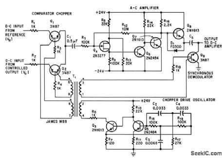


Comporator chopper senses difference between reference voltage and control signal while drowing very little current from reference. Sine-wave drive frequency is determined by C2 and C3, which should have 2 to 1 ratio.-J.S.Mac Dougall,Servo Comparator Amplifier Handles High Voltages,Electronics,37:22.p75-76 (View)
View full Circuit Diagram | Comments | Reading(675)
TRANSIENT_RESPONSE_OF_REGULATED_SUPPLlES
Published:2009/7/11 3:48:00 Author:May

Developed for testing transient response of 12-V regulated power supply at loading of either 100 mA or 1 A,depending on switch position. Load resistors ean be changed for other voltages and currents. Transients generated by supply may be observed on AC-coupled oscilloscope. Good transient response will show only small leading-edge peaks, as in upper waveform. Any tendency of power supply toward instability degrades waveform much more, as in lower diagram. Circuit consists of multivibrator using series diodes in base circuits to protect transistors from excessive voltage swings in switching cycle. Square-wave output is used for oscilloscope trigger and fed to other three transistors that provide load for power supply under tesl.-H. Macdonald, Transient Response Testing, Wireless World, July 1973, p 338. (View)
View full Circuit Diagram | Comments | Reading(679)
Series_shunt_analog_switch_useful_in_applications_requiring_extremely_low_input_to_output_signal_feedthrough_
Published:2009/7/17 2:46:00 Author:Jessie

Series-shunt analog switch, useful in applications requiring extremely low input-to-output signal feedthrough (courtesy Motorola Semiconductor Products Inc.). (View)
View full Circuit Diagram | Comments | Reading(779)
BROADBAND_NE602_INPUT_CIRCUITS
Published:2009/7/17 2:45:00 Author:Jessie

A variety of single-ended input circuits can be used with the NE602,including a broadband capacitor-coupled input and a broadband transformer-coupled input (View)
View full Circuit Diagram | Comments | Reading(712)
AGC_SYSTEM_FOR_CA3028_IF_AMPLIFIER
Published:2009/7/17 2:45:00 Author:Jessie

An MPF102 amplifier feeds IF signals to a 2N4126. A potentiometer in the MPF102 Source acts as agatn control.This voltage is rectified by an 1N914 doubling detector, and drives a 741 op amp vla a source follower(Q14).S-meter and IF-gain controls are provided. (View)
View full Circuit Diagram | Comments | Reading(2468)
TYPEWRITER_KEYS_CW_TRANSMITTTER
Published:2009/7/11 3:47:00 Author:May

Allows operator to send perfect Morse code simply by typing messages on alphameric keyboard. Accuracy is determined only by typing skill of operator. One RC oscillator controls mark-space ratio of Morse characters and duration of character and word spaces, while clock oscillator is divided down and switched to give sendingspeed choices of 6, 12, 24, and 48 words per minute. Each square on keyboard diagram is SPST switch, and each cross at intersection issilicon switching diode such as 1N914. 0utputs of keyboard switches are converted into 15-bit code for feeding into 64-character first-in first-out memory using four MP3812B ICs for storage and for generating corresponding Morse characters. Article gives construction and adjustment details.-C. I. B. Trusson, Morse Keyboard and Memory, Wireless World, Jan. 1977, p 55-59. (View)
View full Circuit Diagram | Comments | Reading(1317)
SCS_PULSE_STRETCHER
Published:2009/7/17 2:45:00 Author:Jessie

Stretch interval is determined by 5-mfd capacitor and 4.7K resistor.- Transistor Manual, Seventh Edition, General Edition Co, 1964, p 435. (View)
View full Circuit Diagram | Comments | Reading(557)
Bistable_switch_using_two_SUS_devices
Published:2009/7/17 2:45:00 Author:Jessie

Bistable (memory) switch using two SUS devices. The mechanical switches can be replaced with other solid-state devices or negative-going pulses referenced to the supply line (courtesy Motorola Semiconductor Products Inc.). (View)
View full Circuit Diagram | Comments | Reading(912)
SIMPLE_AUDIO_FREQUENCY_VCO
Published:2009/7/11 3:47:00 Author:May

The frequency of this sine-wave oscillator is determined by a direct voltage, UC, of 0 to 15 V. The distortion on output signals of up to 10 Vpp is not greater than 1%. When the output is reduced with the aid of Pl to 1 Vpp, the distortion drops to below 0.1% It is not recommended to use output signals below 1 Vpp, because the oscillator then becomes unstable and temperature-dependent.The oscillator consists of two operational transconductance amplifiers (OTAs) contained in one package. Their Amp-bias inputs, pins 1 and 16, are connected in parallel. These inputs can drive the output currents at pins 5 and 12 to a peak value of up to 0.75 mA.Switch S1 enables the oscillator output to be set to two ranges: 6.7 to 400 Hz and 400 Hz to 23.8 kHz.The overall range needs a control voltage that varies from 1.34 to 15 V. When the frequency is changed by a variation of UC and the setting of P1 is not altered, the output signal might be distorted. In other words, the amplitude of the signal must be adapted to the frequency. (View)
View full Circuit Diagram | Comments | Reading(1985)
STRAIN_GAGE_AMPIJFIER
Published:2009/7/17 2:45:00 Author:Jessie

Positive and negative feedback to bridge-type transformer coupled input circuit provides high-impedance looting differential input in d-c to 25-kc amplifier. Bridge balances out commonmode signals that arise in data acquisition systems, where pre-amplifier ground may be hundreds of feet from transducer ground. Floating output delivers low voltage at high current for recorder or analog-to-digital converter. Linearity is within 15 microvolts from d-c to 25 kc. Chopper stabilization keeps input d-c drift below 0.5 microvolt during 40-hour run.-R. S. Burwen, Amplifiers for Strain Gages and Thermocouples, Electron, ics, 32:30, p 43-45. (View)
View full Circuit Diagram | Comments | Reading(853)
DPDT_FET_switch
Published:2009/7/17 2:43:00 Author:Jessie

DPDT FET switch(courtesy Motorola Semiconductor Products Inc.). (View)
View full Circuit Diagram | Comments | Reading(987)
CRYSTAL_TESTER
Published:2009/7/11 3:46:00 Author:May

JFET Pierce oscillator will test any crystal from 50 kHz through 25-MHz upper frequency limit of fundamental-mode crystals without tuning, and drive counter for measuring crystal frequency, Will test overtone VHF crystals on their fundamental frequency. T1 is small output transformer from tube-type radio, having about 33: 1 turns ratio, or 6.3-V filament transformer if 1N645 rectifiers are used in place of 50-μF filter capacitors to give fullwave voltage doubler providing required 9 V. RFC1 is 2.5 mH, and RFC2 is 150-mH miniature toroid.-F. Brown, A Universal Crystal Oscillator, QST, Feb. 1978, p 15-16. (View)
View full Circuit Diagram | Comments | Reading(0)
| Pages:776/2234 At 20761762763764765766767768769770771772773774775776777778779780Under 20 |
Circuit Categories
power supply circuit
Amplifier Circuit
Basic Circuit
LED and Light Circuit
Sensor Circuit
Signal Processing
Electrical Equipment Circuit
Control Circuit
Remote Control Circuit
A/D-D/A Converter Circuit
Audio Circuit
Measuring and Test Circuit
Communication Circuit
Computer-Related Circuit
555 Circuit
Automotive Circuit
Repairing Circuit