
Circuit Diagram
Index 758
TIME_DELAY_USES_POWER_TRANSISTOR_IC
Published:2009/7/12 22:16:00 Author:May

Load is energized when switch is closed C1 charges until voltage across R1 drops below 0.8V、opening LM195 and deenergizing load,Long time delays can be obtained with small capacltor values since high resistance can be used.- Linear Applications,vol 2, National Semiconductor.Santa Clara, CA, 1976,AN-110,p 4. (View)
View full Circuit Diagram | Comments | Reading(765)
CASCADE_WITH_AUTOMATIC_RETRIGGERING
Published:2009/7/12 22:15:00 Author:May

Two timers, each controlling own load andhaving own time intervals (determined by R1C1 and R2C2), recycle automatically when start switch is closed momentarily. If desired, second timer can be set to control ON time offirst timer With 15-V supply, each timer canhandle 200-mA load.-H .Vordenbaum'Automatic Beset Timer,Ham Radio Oct,1974、p50-51. (View)
View full Circuit Diagram | Comments | Reading(549)
MODIFIED_ANALOG_MULTIPLIER
Published:2009/7/17 1:25:00 Author:Jessie
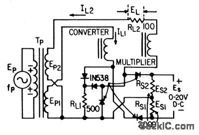
Input signal voltages are obtained from center-tapped 2,000-ohm input resistor so that each signal may change its polarity Circuit then Provides unidirectinal output voltage EL which:is equal to square of ES.J, Markus,” Handbook of Electronic Control Circuits,”McGraw-Hill. N.Y,1959,p 103. (View)
View full Circuit Diagram | Comments | Reading(585)
SPLITTER_CIRCUIT_FOR_ACTIVE_ANTENNA_TO_ENABLE_MULTIPLE_SHORTWAVE
Published:2009/7/12 22:14:00 Author:May

Identical resistor-value star networks can beused to connect multiple receivers to a single active antenna Although the loss is higher with this method than with conventional ferrite transformersplitters,the frequency response goes down to dc.and the extra loss is not usually a problem at LF,MF, and HF, as active antennas have plenty of gain and the received signal levels are limited by at mospherig and ambient noIse signal strengths.The splitter should be mounted in a shielded box with suitable connectors to minimize stray signal pickup. (View)
View full Circuit Diagram | Comments | Reading(772)
5_V_SUPPLY_FROM_THREE_WIRE_RS232_PORT
Published:2009/7/12 22:14:00 Author:May

This circuit produces a semiregulated 5-V output from an RS232 port. The output current-about 8 mA-is sufficient for CMOS microcontrollers and other low-power circuits. IC1 is a switched-capacitor, charge-pump voltage converter that can either invert an input voltage or double it. The connections shown provide a doubler configuration in which the normal input voltage is reversed: A positive input voltage normally connects between GND and OUT, but this circuit connects a negative input between OUT and GND. The IC then doubles the negative Vin the positive direction, producing a positive output (at VDD) equal to [Vin]. The zener diode D1 acts as a shunt regulator that semiregulates Vin to -5 V (actually to -4.7 V). The 33-μF capacitor values shown are larger than normal to support the oqtput voltage during worst-case (all-zero) patterns of transmission. At 9600 baud, for example, an all-zeros character causes an output droop of about 0.2 V. For lower baud rates, substitute a proportionally higher value for C1. (View)
View full Circuit Diagram | Comments | Reading(563)
DC_BLOCK_FOR_ACTIVE_ANTENNA_AND_DOWNCONVERTERS
Published:2009/7/12 22:13:00 Author:May

A suitable dc block and power source for active antennas and downconverters can be made from a few components as shown. This circuit is suitable for frequencies from 50 kHz up to VHF. A shielded case should be employed to prevent stray signal pickup. Dc power supplied to the active antenna or downconverter, via the coaxial signal ca-ble, is 12 V at 30 mA. (View)
View full Circuit Diagram | Comments | Reading(600)
ACTIVE_ANTENNA,100_kHz_TO_30_MHz
Published:2009/7/12 22:12:00 Author:May

This circuit uses a FET and bipolar transistor combination to achieve high performance with a short pickup antenna (24 in. or 70 cm). R5 is a gain control and should be set for the minimum gain necessary for good results. T1 is 24 turns of #32 trifilar wire on a Ferroxcube P/N 768T188-3E2A core. J1 is used for dc feed and RE output. A dc block unit can be used at the receiver end. Dc power is 12 V at 30 mA. The pickup wire and pre-amp should be enclosed in a weatherproof assem-bly so that the antenna can be mounted outdoors in an electrically quiet area.A complete kit of parts, including the PC board, is available from North Country Radio, P.O. Box 53, Wykagyl Station, New Rochelle, NY 10804-0053A.
(View)
View full Circuit Diagram | Comments | Reading(1254)
10_h_DELAYS
Published:2009/7/12 22:12:00 Author:May

Long duration is achieved by separating peak current of timer from charging cuffent. Q1 and R1-R2-R3 form constant-current source whose charging current can be ad justed to as low as several nanoamperes. Q2 acts as source follower to supply current flowing in emitter lead priorto firing of UJT Q3. Diode-con-nected transistor Q1 provides low-impedance discharge path for timing capacitor CE. Delay time varies linearly with setting of R3.- Uni-junction Transistor Timers and Oscillators, Motorola, Phoenix, AZ, 1974, AN-294, p 5. (View)
View full Circuit Diagram | Comments | Reading(549)
12_V_TRANSFORMERLESS_PRENEGULATOR
Published:2009/7/12 22:11:00 Author:May

AC line voltage is converted to regulated 12 VDC by varying firing angle of 10-A SCR. Circuit provides reliable operation for AC line voltages between 50 and 140 V. Key element in trigger-ing of SCR is programmable unijunction transistor that provides variable and accurate control of firing time. Developed for use in power supply that uses digital techniques of sample-and-hold switching to achieve high degrbe of isolation between power line and load without using transformer.-J. A. Dickerson, Transformerless Power Supply Achieves Line-to-Load isolation, EDN Magazine, May 5, 1976, p 92-96. (View)
View full Circuit Diagram | Comments | Reading(2229)
75_W_INSTANT_START_BALLAST_
Published:2009/7/12 22:10:00 Author:May

DC voltage for 20-kHz two-transistor oscillatoris obtained from AC line, Secondaryis added to centertapρed tank coil of T1Bto provide 1 kV P starting voltage required by 96-inch instantstart lamps.Artide gives transformer and choke winding data along with circuit details and performance data. Lamps operate independently, so one stays on when other is removed.-R. J. Haver, The Verdict Is In: Solid-State Fluorescent Ballasts Are Here, EDN Magazine, Nov. 5, 1976, p 65-69. (View)
View full Circuit Diagram | Comments | Reading(805)
PC_IR_CARD_READER
Published:2009/7/12 22:10:00 Author:May


The LED is a high-output infrared emitter. It receives its power through current-limiting resistor R1. With a 9-V power supply and a value of 220 Ω for R1, the diode will receive about 25 mA of current. With a 5-V supply, R1 should be 150 Ω to keep diode current in the 25-mA range. The LED energizes NPN phototransistor Q1, which is configured as a simple inverting amplifier. As more light shines on Q1, the output voltage at its collector decreases. With a value of 2.2 kΩ for R2, the circuit provides TTL-compatible logic levels. The output of Q1 feeds one bit of a PC's parallel port. Diode D2 allows the use of power sources greater than 5 V, thereby maintaining TTL level compatibility-even with high supply voltages. If the voltage at the collector of Q1 ever exceeds 5 V, D2 will block the voltage, thereby protecting the port. On the other hand, when Q1 goes logic low, D2 becomes forward-biased, so the low level can be sensed by the port. (View)
View full Circuit Diagram | Comments | Reading(559)
MAGENTIC_REGISTER
Published:2009/7/12 22:10:00 Author:May

Basis of storage is magetization time.Four ferrite cores will store one deciaml digit under control of one clock pulse.-A.A.Jaecklin.Storing Complete Decimal Digits with One Clock Pulse,Electronice,34:11,p50-53 (View)
View full Circuit Diagram | Comments | Reading(475)
G_M_DRIVE_FOR_SCALE_OF_64_COUNTER
Published:2009/7/17 1:37:00 Author:Jessie

Shapes pulses from Geiger-Muller tube and uses one-shot mvbr to drive first scaling stage.-F. E. Armstrong, Battery Powered Portable Staler, Electronics, 33:19, p 74-75. (View)
View full Circuit Diagram | Comments | Reading(536)
HIGH_FREQUENCY_LOOP_ANTENNA
Published:2009/7/12 22:10:00 Author:May

Good performance in the 5- to 30-MHz range requires an amplifier with extremely high input im-pedance and low noise that can drive 75-Ω loads at high signal levels at frequencies over 30 MHz.Combining dual FET source followers and the new Maxim 436 wideband transconductance amplifier can produce just such an amplifier. A balanced configuration is used for the tuned loop to preserve the symmetry of the figure-eight polar antenna pattern. As a result of using FET source followers on the amplifier's front end, only the 1-MΩ gate resistors load the tuned circuit, so tuning is very sharp and resistance to off-frequency interference is very high. The FETs drive the differential inputs of the MAX436, which amplifies the balanced signal and converts it to a single-ended output. Voltage gain for this amplifier is switch selectable at either 8 dB or 20 dB into a 75-Ω load. Since the ampli-fier is designed to work into a 75-Ω load, the device can be connected to the receiver with a length of RG-59U cable. Maximum undistorted output is 1500 mV into 75 Ω, so overloading is unlikely even at the high-gain setting. (View)
View full Circuit Diagram | Comments | Reading(1853)
10_s_TIMER
Published:2009/7/12 22:09:00 Author:May

CA3096 transistor array provides all needed active devices, 5-μF capacitor charges through Q4 until it turns on bistable switch Q1-Q2, which then triggers Q3 to deliver current to lamp load to indicate end of timing interval.- Circuit ldeas for RCA Linear ICs, RCA Solid State Division, Somerville, NJ, 1977, p8.
(View)
View full Circuit Diagram | Comments | Reading(836)
MINI_HIGH_VOLTAGE_PROBE
Published:2009/7/17 1:37:00 Author:Jessie

The schematic diagram of the probe reveals its simple circuit. It is a standard voltage divider made up of resistors with a 1-percent tolerance. Resistors R1 and R2 are the key elements here. They are rated at 15,000 V and 10,000 V, respectively. The 7500-Vdc peak specification for the assembled probe must not be exceeded under any circumstances! The values for series resistors R3 and R4 are in parallel with the 10-MΩ resistance of the DVM, thus providing a 1000-to-1 voltage divider. Voltage measurements made by the probe should be multiplied by a factor of 1000. If your DVM uses an input impedance different from the standard 10 MΩ, you can adjust the R3/R4 series combination, as needed. (View)
View full Circuit Diagram | Comments | Reading(960)
±12_V
Published:2009/7/17 1:36:00 Author:Jessie


Simple circuit provides power required for two 741 opamps used in CRT tuning indicator circuit for RTTY receiver.-R. R. Parry, RTTY CRT Tuning Indicator, 73 Magazine, Sept. 1977, p 118-120. (View)
View full Circuit Diagram | Comments | Reading(1130)
PREFERRED_PULSE_SHAPER
Published:2009/7/17 1:36:00 Author:Jessie

Generally used with monostable mvbr to form 1-microsec pulse at end of delay period. Also used to reshape pulse that has suffered deterioration by passage through long chain of gates, or to produce 1.microsec pulse whose leading edge coincides with trailing edge of a positive pulse, for delaying output by width of input pulse.-NBS, Handbook Preferred Circuits Navy Aeronautical Electronic Equipment, Vol. 11, Semiconductor Device Circuits, PSC 11 (originally PC 214), p 11-2. (View)
View full Circuit Diagram | Comments | Reading(673)
ACTIVE_DIPOLE_ANTENNA
Published:2009/7/12 22:07:00 Author:May

This active antenna acts as a dipole and consists of a dual FET source follower feeding a differential amplifier. The LM759 acts as a virtual ground, splitting the 10-V supply. R1 is a gain set resistor (see table). Dc is fed in via coax cable. The frequency range is 100 kHz to 40 MHz. (View)
View full Circuit Diagram | Comments | Reading(2890)
LOGIC_PROBE_
Published:2009/7/17 1:34:00 Author:Jessie

The figure shows the schematic for a versatile logic probe. The zener diode clamps the input signal just above the TTL inverter's 2.2-V trigger voltage. Zener diode D1 can be left out if the probe is going to be used only on TTL circuits. The logic probe is based mainly on inverters IC1-a and IC1-b, which are sections of a 7404 integrated circuit. Depending on whether the input is high or low, the inverters enable AND gate IC2-a or IC2-b, each of which is a section of a 4081. Each AND gate is connected to an oscillator, one low-frequency, the other high. When an AND gate is made high, it passes the frequency of its oscillator to the piezo buzzer (BZ1). Whenever a high is at the input, the buzzer will produce the high tone; whenever a low is at the input, the buzzer will sound the low tone. With switch S2 in the PULSE position, if pulses are present at the input, a yellow LED will light and the buzzer will sound at the frequency of the pulses. The CMOS/TTL switch selects the voltage from the circuit under test or the voltage from the 78L05 regulator. Note that when this switch is in the TTL position, it can work only with 5-Vdc, but when the switch is in the CMOS position, it can work with from 7.5 to 35 Vdc. (View)
View full Circuit Diagram | Comments | Reading(3885)
| Pages:758/2234 At 20741742743744745746747748749750751752753754755756757758759760Under 20 |
Circuit Categories
power supply circuit
Amplifier Circuit
Basic Circuit
LED and Light Circuit
Sensor Circuit
Signal Processing
Electrical Equipment Circuit
Control Circuit
Remote Control Circuit
A/D-D/A Converter Circuit
Audio Circuit
Measuring and Test Circuit
Communication Circuit
Computer-Related Circuit
555 Circuit
Automotive Circuit
Repairing Circuit