
Circuit Diagram
Index 747
NEON_TUBE_HIGH_VOLTAGE_POWER_SUPPLY
Published:2009/7/16 21:58:00 Author:Jessie
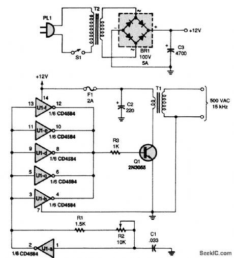
Power for the circuit is supplied by a step-down transformer (T2) and a full-wave bridge rectifier (BR1), which convert 117-Vac to 12-Vdc. Capacitor C3 acts as a filter. The heart of the circuit is a Schmitt-trigger hex inverter, U1. Capacitor C1, resistor R1, and potentiometer R2 are connected to one section of the inverter, U1-a, to form an oscillator that runs at approximately 15 kHz (because U1 is a Schmitt trigger, the output square wave is very clean). Adjusting R2 varies the frequency. The output of the oscillator is fed into the remaining five inverters (U1-b through U1-f), which are connected in parallel to create a buffer that is capable of increasing the drive current of the oscillator. The square-wave output is used to drive the switching transistor (Q1), which, in turn, switches the primary windings of the ferrite-core transformer (T1). Approximately 500-Vac at 15 kHz are output from the secondary of the transformer. T1 is made from a ferrite pot core. Wind 500 turns of #30-gauge wire for the secondary. Coat it with insulating varnish and add a layer of insulating tape, over which a 20-turn winding of #22 wire is wound to form the primary winding. (View)
View full Circuit Diagram | Comments | Reading(2293)
Bile Former Grade Circuit Of Good Performance
Published:2011/7/17 23:41:00 Author:Felicity | Keyword: Bile Former Grade, Good Performance

View full Circuit Diagram | Comments | Reading(1004)
IMPROVED_CLIPPING_CIRCUIT_DESIGN
Published:2009/7/16 21:58:00 Author:Jessie
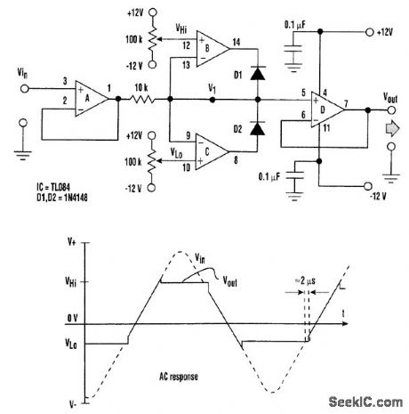
Op amps A and D form unity-gain buffer amplifiers. Op amps B and C compare the input voltage (Vin) with the reference voltages (VHi and VLo). These references set the high and low clipping levels of the circuit. When the input voltage lies in the range (VHi-VLo), the outputs of the comparators make both diodes (D1 and D2) reverse-biased. As a result, the circuit's output Vout follows the input voltage. When the input voltage exceeds the value VHi op amp B's output goes negative, forward-biasing D1 and thus reducing V1 the voltage at the invertinginput of op amp B. The circuit reaches an equilibrium condition at which Vout=V1=VHi Similarly, when the input voltage goes below the value VLo, op amp C's output goes positive, forward-biasing D2. This increases the voltage at V1, At the equilibrium condition, Vout=V1=VLo. The circuit's output continues to follow the input for about 2μs, even after the input voltage crosses the reference voltages, because of the slew rates of the op amps.The supplies (5V≤V+≤15V, -5V≥V-≥-15 V). (View)
View full Circuit Diagram | Comments | Reading(1364)
12_AND_5_V
Published:2009/7/16 21:57:00 Author:Jessie
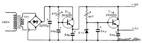
Used with multiple photographic development timer to provide 12 V at about 5mA and 5 V at about 300mA for logic, control, and audible alarm circuits.-R. G. Wicker, Photographic Development Timer, Wireless World, April 1974, p 87-90. (View)
View full Circuit Diagram | Comments | Reading(644)
HV_POWER_SUPPLY
Published:2009/7/16 21:56:00 Author:Jessie
This power supply uses a Cockcroft-Walton HV multiplier circuit to produce up to 10 kV from a 12-V source. Up to 5 W is available from this circuit. (View)
View full Circuit Diagram | Comments | Reading(2347)
S812/S802 series adjustable regulator output voltage circuit diagram
Published:2011/7/20 5:18:00 Author:nelly | Keyword: regulator, output voltage
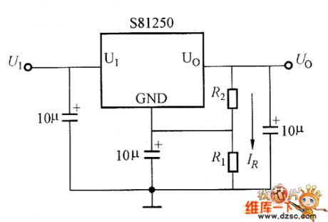
View full Circuit Diagram | Comments | Reading(1349)
±6_V_AND_±12_V
Published:2009/7/16 21:56:00 Author:Jessie

Provides regulated power required by 5-MHz frequency standard and its temperature-controlled crystal oven. Current is measured by switching milliammeter and series resistor across current-limiting resistors R3 and R10, which also serve as meter shunts. DC input voltage at terminal 3 of MC1460R regulator should be at least 3 V greater than output voltage but should not exceed 20-V rating. Adjust R5 and R12 as required to get correct output voltages. Diodes ale 200 PIY at 0.5 A. T1 and T2 have 117-V primary and 25.2-V secondary at 0.3 A, T3 has 117-V primary and 6.3-V secondary at 1 A.-R. Silberstein, An Experimental Frequency Standard Using ICs, QST, Sept. 1974, p 14-21 and 167. (View)
View full Circuit Diagram | Comments | Reading(860)
ALPHANUMERIC_CHARACTER_GENERATOR
Published:2009/7/16 21:55:00 Author:Jessie

Used to Provide readout on cathode-ray display as output of digital computer. Horizon-tal decoding and deflection circuits are shown.240 Vertical circuitry is essentially identical.-E.D. Jones, Character Generator for Digital Computers,Electronics,33:7, p 117-120. (View)
View full Circuit Diagram | Comments | Reading(1030)
SCHMIDT_TRIGGER_MEMORY_CELL_CIRCUIT
Published:2009/7/16 21:55:00 Author:Jessie

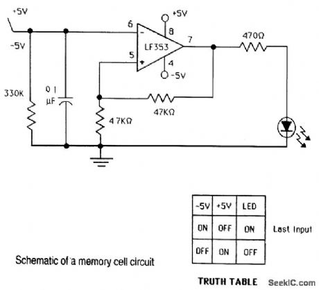
View full Circuit Diagram | Comments | Reading(911)
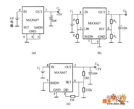
ADP667 adjustable output voltage circuit diagram
Published:2011/7/20 5:20:00 Author:nelly | Keyword: adjustable output voltage

View full Circuit Diagram | Comments | Reading(668)
ADP667 5V fixed voltage output circuit diagram
Published:2011/7/20 5:21:00 Author:nelly | Keyword: fixed voltage output

View full Circuit Diagram | Comments | Reading(880)
5_V_AT_1_A
Published:2009/7/16 21:54:00 Author:Jessie

Can handle over 30 TTL ICs in frequency counter if LM309K regulator is mounted directly on aluminum heatsink. Case of regulator is grounded, so mica insulation is not needed. Provides excellent regulation with practically no output ripple and is short-circuit-proof. Circuit also shuts itself off if temperature gets too high. - P. A, Stark, A Simple 5 V Power Supply for Digital Experiments, 73 Magazine, Oct. 1974, p 43-44. (View)
View full Circuit Diagram | Comments | Reading(0)
MAX667 application circuit diagram
Published:2011/7/20 5:22:00 Author:nelly | Keyword: application
View full Circuit Diagram | Comments | Reading(940)
SHOCK_EXCITED_COSINE_WAVE_OSCILLATOR
Published:2009/7/16 21:53:00 Author:Jessie

Single 34.1-mlcrosec ring command turns on five identical harmonic generators for alphanumeric character generator.-K. E. Perry and E. J. Aho,Radar-Computer Display Traces Alphanumeric Characters, Electronics, 34:26, p 75-79. (View)
View full Circuit Diagram | Comments | Reading(669)
5V fixed voltage output circuit diagram
Published:2011/7/20 5:23:00 Author:nelly | Keyword: 5V voltage output, fixed voltage output

View full Circuit Diagram | Comments | Reading(620)
±15_V_1
Published:2009/7/16 21:53:00 Author:Jessie

Developed for use in two-tone AF generator for testing SSB equipment. BR1 is Motorola HEP176 or MDA-920. U2 is Raytheon 4195DN.-H. Olson, A One-Chip, Two Tone Generator, CQ, April 1974, p 48-49. (View)
View full Circuit Diagram | Comments | Reading(700)
CHARACTER_DEFLECTION_AMPLIFIER
Published:2009/7/16 21:52:00 Author:Jessie

Converts X or Y voltage waveform into equivalent current waveform of up to 0.5 amp peak to peak, to drive low-inductance defection yoke of cathode-ray character generator.-K. E. Perry and E. J. Aho, Radar. Computer Display Traces Alphanumeric Characters, Electronics, 34:26, p 75-79. (View)
View full Circuit Diagram | Comments | Reading(774)
SHOCK_EXCITED_SINE_WAVE_OSCILLATOR
Published:2009/7/16 21:51:00 Author:Jessie

Rectangular pulse turns on five identical harmonic generators for alphanumeric character generator.-K. E. Perry and E. J. Aho, Radar-Computer Display Traces Alphanumeric Charactors, Electronics, 34;26, p 75-19. (View)
View full Circuit Diagram | Comments | Reading(722)
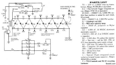
JACOBS_LADDER_HV_SUPPLY
Published:2009/7/16 21:51:00 Author:Jessie

The operation of the Jacobs's Ladder depends on the current-limited power supply that delivers 12,000 V at 40 mA from the 120-Vac line. The full-wave bridge BR1 rectifies the 120-Vac line input, and resistor R1 limits the dc charging current of capacitor C3 to a safe value. The drive circuit power is obtained by dropping the 120-Vac line through capacitor C4 and current-limiting resistor R2. Capacitor C4 and resistor R2 present a complex impedance, so most of the ac line voltage is dropped across the reactance. The 555 timer IC is configured as a square-wave oscillator. The output frequency of its square waves is determined by the setting of trimmer potentiometer R5 and capacitor C6. The frequency is about 25 kHz for the values of R5 and C6 shown. Potentiometer R5 can be used to adjust the circuit's power output. Increasing the frequency reduces the circuit's output by increasing the inductive reactance of the transformer leakage inductance. The output of IC1 on output pin 3 appears at the bases of the current source, NPN transistor Q1, and sink, PNP transistor Q2. The emitters of this transistor pair are ac-coupled through capacitor C8 and resistor R6 to drive the primary of driver-isolation transformer T1. This drive prevents dc from flowing through the primary. Transformer T1 is wound on a high-permeability core with as few turns as possible to eliminate leakage inductance. The gate circuits of MOSFETs Q3 and Q4 contain 27-Ω resistors (R7 and R9) to slow their switching times. This eliminates possible parasitic oscillations that could occur if the MOSFETs were switched at their speed limit. The primary of output transformer T2 contains 32 turns, but its secondary contains 2500 turns. The ratio of these turns is approximately 1 to 78. When this is multiplied by the rectified line voltage of 160 Vdc, an output of about 12,000 peak volts is obtained across the secondary. This 12,000-V output is the peak open-circuit voltage of the system, and it produces a short-circuit current of approximately 40 mA. This current is limited by the leakage inductance caused by the loose magnetic coupling between the primary and secondary circuits of transformer T2. (View)
View full Circuit Diagram | Comments | Reading(3483)
CHARACTER_GENERATOR_DEFLECTION_SWITCH
Published:2009/7/16 21:50:00 Author:Jessie

Coarse deflection system uses 32 identical power transistor circuits in switching configuration to drive low-inductance main deflection yoke. Half of these control X deflection to give 16 discrete positions, and the remainder serve for Y deflection.-K. E. Perry and E. J. Aho, Radar-Computer Display Traces Alphanumeric Characters,Electronics, 34:26, p 75-79. (View)
View full Circuit Diagram | Comments | Reading(755)
| Pages:747/2234 At 20741742743744745746747748749750751752753754755756757758759760Under 20 |
Circuit Categories
power supply circuit
Amplifier Circuit
Basic Circuit
LED and Light Circuit
Sensor Circuit
Signal Processing
Electrical Equipment Circuit
Control Circuit
Remote Control Circuit
A/D-D/A Converter Circuit
Audio Circuit
Measuring and Test Circuit
Communication Circuit
Computer-Related Circuit
555 Circuit
Automotive Circuit
Repairing Circuit