Basic Circuit
Discharge type single trigger timing circuit formed by PUT
Published:2011/8/2 5:14:00 Author:Nancy | Keyword: Discharge type, single trigger , timing | From:SeekIC
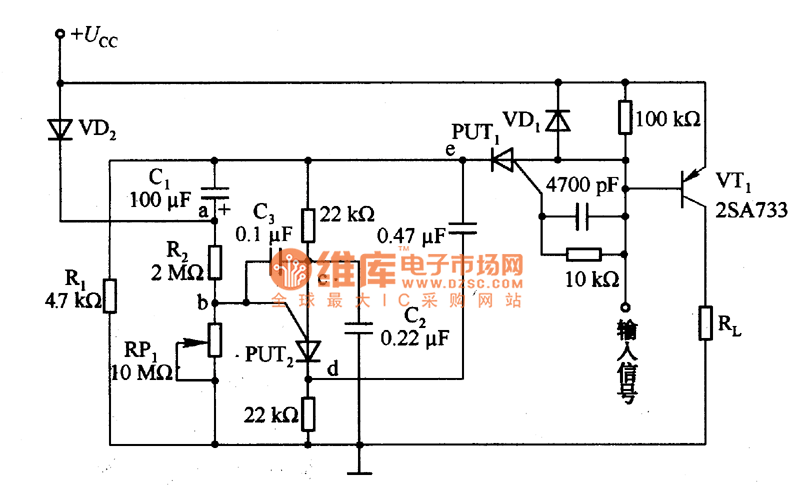
Figure 1 is the discharge type single trigger timing circuit formed by PUT. When there is no input signal, PUT1 cuts off, and so does the transistor VT1. At this time, C1 charges to the power supply voltage Ucc. If we add the input signal, PUT1 and VT1 conduct, current flows through the load RL. At the same time, the potential of point a is two times of the power supply voltage Ucc, C2 and C3 charge to the power supply voltage Ucc. From this time, C1 discharges through R2 and RP1, then the potential of point a drops slowly. After reaching the set time, if the potential of point b is lower than that of point c, then PUT conducts.
Reprinted Url Of This Article:
http://www.seekic.com/circuit_diagram/Basic_Circuit/Discharge_type_single_trigger_timing_circuit_formed_by_PUT.html
Print this Page | Comments | Reading(3)

Article Categories
power supply circuit
Amplifier Circuit
Basic Circuit
LED and Light Circuit
Sensor Circuit
Signal Processing
Electrical Equipment Circuit
Control Circuit
Remote Control Circuit
A/D-D/A Converter Circuit
Audio Circuit
Measuring and Test Circuit
Communication Circuit
Computer-Related Circuit
555 Circuit
Automotive Circuit
Repairing Circuit
Code: