Basic Circuit
Timing circuit formed by PUT
Published:2011/8/2 19:44:00 Author:Nancy | Keyword: Timing circuit, PUT | From:SeekIC

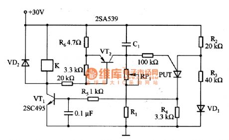
Figure 1 is the timing circuit formed by PUT. It is a 0.5s一lmin time variable timing circuit composed by PUT. The anode-cathode of PUT is offset by the voltage division of fixed resistors R2 and R3, the timing is decided by the capacitor C1 and resistor (R(RP1)十R1) connected to the gate. The base current of the drive transistor VT1 of the relay K is decided by the R2, R4 and R5, it is not relevant to the timing setting resistor for the PUT conduction. The electric charge of capacitor C1 discharges through VT2 and R6, the diode VD1 used to compensate the temperature characteristic of PUT.
Reprinted Url Of This Article:
http://www.seekic.com/circuit_diagram/Basic_Circuit/Timing_circuit_formed_by_PUT.html
Print this Page | Comments | Reading(3)

Article Categories
power supply circuit
Amplifier Circuit
Basic Circuit
LED and Light Circuit
Sensor Circuit
Signal Processing
Electrical Equipment Circuit
Control Circuit
Remote Control Circuit
A/D-D/A Converter Circuit
Audio Circuit
Measuring and Test Circuit
Communication Circuit
Computer-Related Circuit
555 Circuit
Automotive Circuit
Repairing Circuit
Code: