
Circuit Diagram
Index 724
TWO_INDEPENDENT_DELAYS
Published:2009/7/13 2:26:00 Author:May
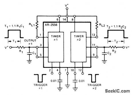
Each timer section of Exar XR-2556 dual timer operates independently in mono MVBR mode to provide delays shown above output waveforms Supply voltage range is 4.5 to 16 v.-Timer DataBook, Exar Integrated Systems, Sunnyvale,CA,1978,p23-30. (View)
View full Circuit Diagram | Comments | Reading(512)
1_min_WITH_TRANSISTOR_ARRAY
Published:2009/7/13 2:24:00 Author:May
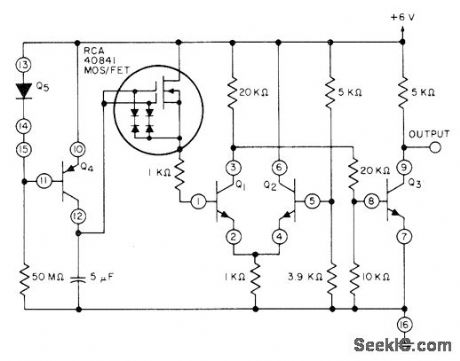
Circuit uses RCA CA3096AE five-transistor array in combination with dual-gate MOSFET to provide timing action that maintains accuracy within 7% for supply voltage variations of ±10%, Q5 is one of PNP transistors connected as diode.- Linear Integrated Circuits and MOS/FET's, RCA Solid State Division, Somerville, NJ, 1977, p 205-210. (View)
View full Circuit Diagram | Comments | Reading(753)
40_V_INPUT_5_C_10_A_DC_TO_DC_CONVERTER
Published:2009/7/13 2:23:00 Author:May


Generating 5 V at 10 A from a 40-V supply with up to 90 percent efficiency is possible using a synchronous switching regulator. The synchronous switching regulator circuit shown achieves this high efficiency by using external MOSFETs with low RDS(ON) and by shunting the Schottky diode after the topside MOSFET has completely turned off to minimize the Schottky diode's conduction losses. The LT1160 half-bridge driver alternately drives the high side and low side MOSFETs ON and OFF during switching. The loop is controlled by the LT3846 current-mode PWM controller and operates at 40 kHz. A key feature of this circuit is the ability to drive the external high-current MOSFETs safely. Internal logic in the LT1160 prevents both MOSFETs from being on at the same time, and its unique adaptive protection against shoot-through currents eliminates all matching requirements for the external MOSFETs. These protection features, in combination with the LT1160's ability to drive up to 10,000 pF of gate capacitance, make paralleling power MOSFETs for high-current applications an easy task. The high-side gate voltage is provided by a floating supply, which is boosted above the HV rail by bootstrap capacitance Cboost. An undervoltage detector in the LT1160 can sense an undervoltage condition at either the input supply or the floating supply and turn off both MOSFETs to prevent excessive power dissipation. (View)
View full Circuit Diagram | Comments | Reading(678)
CURRENT_LIMITERS
Published:2009/7/13 2:23:00 Author:May

A user-controlled internal current limit on power op amps isn't always provided by manufacturers. However, the current limit can be set extemally by using the technique shown, in which the output current is sensed with a single resistor. The resistor activates a complementary transistor switch that reduces irtverting gain, lirrtiting output current. The technique is demonstrated with 8-pin OPA2541 or OPA2544 dual-power op amps that are lacking an intemal user-controlled current limit. The extemal components add an adjustable current limit to these amplifiers. The PNP transistor controls the positive current limit, and the NPN transistor controls the negative current limit. Both transistors are 0FF until the voltage drop across RCT reaches the current-limit set point. At the current-limit set point, current from the controlling transistor will sum with the input current (through Ri) at the op amp's inverting input summing junction. This will limit the output. The diodes in series with the collectors of both transistors prevent forward base-collector bias. High-frequency oscillation during current limit is damped out with the 1000-pF capacitors. These capacitors only nominally affect the conftguration's closed-loop bandwidth because the diodes, which are normally off, isolate them. (View)
View full Circuit Diagram | Comments | Reading(1047)
LOW_STANDBY_DRAIN
Published:2009/7/13 2:23:00 Author:May
Positive 12-V pulse at input A triggers SOS Q1 and turns on transistor switch Q3, Positive pulse at input B gates SCS Q2 on and turns off Q3. Current drain is essentially zero (typically 3 μA). Circuit was designed to supply up to 7 mA of switched current from 12-VDC supply.-D. B. Heckrnan, Bistable Switch with Zero Standby Drain, EDN|EEE Magazine, Oct. 1, 1971, p 42. (View)
View full Circuit Diagram | Comments | Reading(583)
MACHINE_GUN_CONTROL_OSCILLATOR
Published:2009/7/13 2:22:00 Author:May

Phase-shift oscillator firing circuit for airborne 20-mm guns permits operation anywhere in range of 600 to 900 rounds per minute,Accuracy is improved by adjusting firing rate away from natural gun-mount vibration frequency.-M. Halio, Firing Circuits Trigger Airborne Machine Guns, Electronics, 31:31, p 86-89. (View)
View full Circuit Diagram | Comments | Reading(883)
CAR_STEREO_SUBWOOFER_CROSSOVER
Published:2009/7/13 2:21:00 Author:May
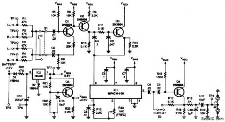
This figure is the schematic for the subwoofer crossover. The inputs through Q1 form a differential summing amplifier, with switch S1 functioning as a polarity inverter. A 24-dB-peroctave switched capacitor filter (IC1) is the heart of the continuously variable filter. Potentiometer R13 controls the cutoff frequency of IC1 by controlling its sampling frequency. Because of the in-herent sampling action of switched capacitor filters, an antialiasing filter is required at the input of IC1. Transistors Q2 and Q3, along with the surrounding components, form this second-order low-pass antialiasing filter. The subsonic filter with a boost stage follows the output of IC1 at 5. When switch S2 is closed, the boost is added. Additional subsonic filtering action is provided by C1 and C2 at the inputs of the crossover circuit. A reconstruction filter that eliminates sampling artifacts is formed by R18 and C10 at the output of IC1. The power-supply circuit, based on the 78L08 voltage regulator (IC2), provides both an 8.6-V main supply and a 4.8-V bias supply. Diode D1 protects against negative voltage spikes and incorrect hookup. Diode D2 biases the 78L08 regulator reference pin at 0.6 V to provide an output of 8.6 V, rather than 8 V. (View)
View full Circuit Diagram | Comments | Reading(2426)
5_V_TO_12_V_1_A_DC_TO_DC_CONVERTER
Published:2009/7/13 2:19:00 Author:May
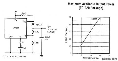
Local on-board conversion from 5 V to 12 V for use in amplifier, signal conditioning, or bus driver circuitry normally entails the use of a module or complex dc-to-dc converter design. The LT1269 100-kHz PWM switching regulator can provide a minimum of 1 A at a regulated 12 V in a surface-rnountable DD package (500 mA in 20-lead, small-outline SMT). Included on the chip is a low-ON-resistance switch (0.33 Ω) with a 4-A current limit for high-efficiency conversion in the boost converter shown here. The high switching frequency permits the use of small inductors and capacitors in this converter. The device can be placed in a micropower shutdown mode (100 μA typical supply current) by activating a clamp on the VC pin. (View)
View full Circuit Diagram | Comments | Reading(825)
HIGH_GAIN_AMPLIFIER_FOR_PHOTODETECTORS
Published:2009/7/13 2:19:00 Author:May
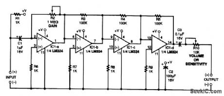
Suitable for photodetectors, laser experiments, or general use, single LM324 quad op amp. A 9-V supply is recommended. (View)
View full Circuit Diagram | Comments | Reading(1305)
POWERED_SUBWOOFER
Published:2009/7/13 2:18:00 Author:May

The power supply consists of a center-tapped 48-V transformer, a bridge rectifier, and filter capacitors. The rectified and filtered output is about ±35 V. The power supply for op amp IC1 is regulated to ±15 V by zener diodes D1 and D2 and resistors R19 and R20. The input circuit consists of a mixer and voltage divider formed by resistors R1 and R2, potentiometer R3, and unity-gain buffer IC1-a. Potentiometer R3 is provided to adjust the output of the subwoofer to the desired level. Op amp IC1-b provides a 12-dB-peroctave high-pass filter with capacitors C2 and C3 and resistors R5 and R6. The cutoff frequency for this filter is 1/2πRC, or about 34 Hz with the values shown. Resistors R8 and R7 set the gain and Q of the filter. Capacitor C1 and resistor R4 form an additional 6-dB-peroctave high-pass filter at about 20 Hz. A 12-dB-peroctave low-pass filter is formed by IC1-c, C4 and C5, and R9 and R10. The values shown set the low-pass cutoff at 72 Hz. The gain and Q of this stage are set by R11 and R12. These two filters, connected back-to-back, form a bandpass filter. When operated with ±15-V supplies, the output of op amp IC1-d can swing about 10 V peak to drive transistors Q1 and Q2. Resistors R17 and R18 provide negative feedback, and set the gain of the out-put stage at about 3. Hence, the output can swing to about 30 V peak. As long as the transistors are the high-beta types specified, the peak power output into an 8-Ω load is (30×30/8)/2556 W rms. The overall gain of the amplifier is set by resistor R13 and feedback resistor R14. (View)
View full Circuit Diagram | Comments | Reading(5147)
HIGH_CURRENT_5_V_TO_12_V_25_A_DC_TO_DC_CONVERTER
Published:2009/7/13 2:16:00 Author:May
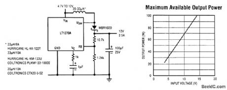
Many applications require a 12-V supply for control, data storage, interface, or driver functions.These designs often require high peak currents, and a 12-V supply might not be available with high enough current. The LT1270A circuit shown here will provide a minimum of 2.5 A at 12 V from a 5 V ±5 percent supply. The LT1270A has a 10-A high-efficiency switch and a low 10-mA (maximum) supply current, which provides excellent efficiency in high-current-output dc-to-dc conversion circuits. The 60-kHz swttcittng frequency has been optimized for best efficiency. (View)
View full Circuit Diagram | Comments | Reading(676)
REMOTE_DIGITAL_PROGRAMMING_OF_TIMER
Published:2009/7/13 2:16:00 Author:May

Either binary or BCD logic can be used for selecting delay interval of monostable timer A1, with delays being integral multiples of shortest time. Timing is programmed by pair of 4016 CMOS analog switches, A2 and A3. Given timing tap is activated when corresponding digital input control line is high and deactivated when control is low. Programmable timing range is 1 to 255 ms for 2240, and 1 to 99 ms for 2250 or 8250 timer. Basic interval can bechanged to suit other applications. CMOS output buffer stage ensures valid output logic Ievels. Although circuit will operate over supply range indicated, operation is optimum forsupply of 10 to 15V.-W. G. Jung, Take a Fresh Look at New IC Timer Applications, EDN Magazine, March 20, 1977, p 127-135. (View)
View full Circuit Diagram | Comments | Reading(669)
CURRENT_DIFFERENCE_AMPLIFIER_USAGE_CIRCUITS
Published:2009/7/13 2:15:00 Author:May
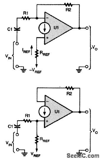
Here a current difference amplifier is used much like an op amp in an inverting follower circuit.Here is a noninverting follower built around a current difference amplifier. (View)
View full Circuit Diagram | Comments | Reading(575)
2500V_AT_500_mA
Published:2009/7/13 2:15:00 Author:May
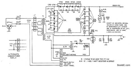
Meets power requirements for 2-kW linear amplifier using pair of 8873 conduction-cooled triodes fol SSB transmitter service. Power transformer is Hammond 101165.Diodes are 1000 PIY at 2.5A,such as Motorola HEP170.T2 is Stancor P-8190 rated 6.3 V at 1.2A.DS1 is 117-V neon pilot lamp Set tap on R1 5000 ohms from B-lead Make adjustments only after tuming off power and allowing time for capacitors to discharge; output voltages are dangerous.-R. M. Myers and G. Wilson, 8873s in a Two-Kilowatt Amplifier, QSL Oct. 1973, p 14-19.
(View)
View full Circuit Diagram | Comments | Reading(1261)
500_kHz_5_V_TO_12_V_400_mA_DC_TO_DC_CONVERTER
Published:2009/7/13 2:14:00 Author:May

In some 5-V-only systems, it is necessary to generate a local 12-V supply to power op amps, data-acquisition circuitry, or devices, such as small motors. The LT1372 is a 500-kHz high-efftciency switching power regulator that provides this capability, as shown in this circuit. The 500-kHz switching frequency reduces the size of the magnetics significantly over that in lower-frequency designs; they consume just 0.5 in2 oftotal board space. The internal switches are current-limited to 1.5 A. In addition, the quiescent current gf LT1372 is just 4 mA, which, along with very low switch losses, provides up to 89 percent efficiency in this application. Other features of the LT1372 include synchronization of the switching action to a system clock source and shutdown capability, reducing supply currents to just 12 μA. Also, the LT1372 has two feedback inputs that allow regulation of either positive or negative output voltages. (View)
View full Circuit Diagram | Comments | Reading(1051)
OVER_1_min
Published:2009/7/13 2:14:00 Author:May

Circuit provides delays well over 1 min even with low operating voltages of ICs. When start pulse is applied to RS flip-flop A1-A2, Q2 turns off and allows RT to provide charging current for timing capacitor CT. When voltage across CT gets high enough, Q1 turns on and resets flip-flop, terminating delay period. A3 provides buffered complementary output.-R. W. Hilsher, Long-Delay Timer, EEEMagazine, Aug. 1970, p 79.
(View)
View full Circuit Diagram | Comments | Reading(724)
Voltage negative feedback offset circuit diagram
Published:2011/7/18 10:36:00 Author:Nancy | Keyword: negative feedback, offset circuit
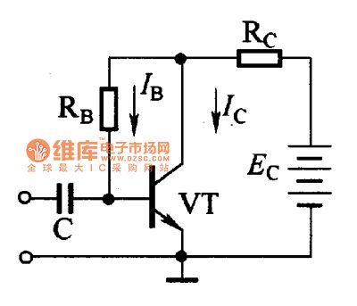

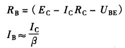

The voltage negative feedback offset circuit is shown as the figure. The bias resistor RB is connected to the transistor collector, which is the difference between it and the fixed offset circuit. At this time the parameters in the circuit has the following relations:
Because the UBE is very small and can be ignored, at this time
The process of steady working point of the circuit is as below:
From the above process, you can see that the change of IC is back along with the increase of temperature, which realizes the role of stabilizing the static working point.
To make the the effect of the circuit excellent, you must make RC large enough, only this can cause the UCE change much and deepen the effect of the voltage negative feedback. So this circuit is not suitable for the circuit which uses the transformer as load. Drift resistance value (2~ 1 O) is often chosen as Rc. (View)
View full Circuit Diagram | Comments | Reading(743)
CURRENT_DIFFERENCE_AMPLIFIER
Published:2009/7/13 2:14:00 Author:May
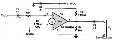
This practical 20-dB gam ac amplifier uses the LM3900 CDA. (View)
View full Circuit Diagram | Comments | Reading(673)
LM3900_AC_AMPLIFIER
Published:2009/7/13 2:12:00 Author:May
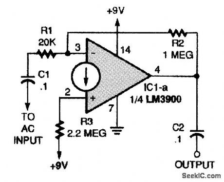
Although the LM3900 current difference amplifier (IC1) used in this ac amplifier really isn't a true op amp, it does simulate one in its performance; however, the IC requires only a one-polarity power source.Gain is R2/R1, and R3 is 2×R2. (View)
View full Circuit Diagram | Comments | Reading(1670)
FET_TIMER_WITH_RELAY
Published:2009/7/13 2:12:00 Author:May

With values shown, circuit gives delay of several seconds. Increas-ing C1 bv shunting with 20-μF capacitor delays energizing of relay to over 1 min. C1 is charged to -4.5 V when switch S1 is closed, biasing gate to cutoff and deenergizing relay. When S1 is open, capacitor begins discharging at rate determined by RC time constant of circuit. When voltage across capacitordrops to point at which 01 conducts, relay is energized and power is applied to load.-E. M. Noll, FET Principles, Experiments, and Projects, Howard W. Sams, Indianapolis, IN, 2nd Ed., 1975, p 215-216. (View)
View full Circuit Diagram | Comments | Reading(1135)
| Pages:724/2234 At 20721722723724725726727728729730731732733734735736737738739740Under 20 |
Circuit Categories
power supply circuit
Amplifier Circuit
Basic Circuit
LED and Light Circuit
Sensor Circuit
Signal Processing
Electrical Equipment Circuit
Control Circuit
Remote Control Circuit
A/D-D/A Converter Circuit
Audio Circuit
Measuring and Test Circuit
Communication Circuit
Computer-Related Circuit
555 Circuit
Automotive Circuit
Repairing Circuit