Basic Circuit
Voltage negative feedback offset circuit diagram
Published:2011/7/18 10:36:00 Author:Nancy | Keyword: negative feedback, offset circuit | From:SeekIC

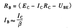


The voltage negative feedback offset circuit is shown as the figure. The bias resistor RB is connected to the transistor collector, which is the difference between it and the fixed offset circuit. At this time the parameters in the circuit has the following relations:
Because the UBE is very small and can be ignored, at this time
The process of steady working point of the circuit is as below:
From the above process, you can see that the change of IC is back along with the increase of temperature, which realizes the role of stabilizing the static working point.
To make the the effect of the circuit excellent, you must make RC large enough, only this can cause the UCE change much and deepen the effect of the voltage negative feedback. So this circuit is not suitable for the circuit which uses the transformer as load. Drift resistance value (2~ 1 O) is often chosen as Rc.
Reprinted Url Of This Article:
http://www.seekic.com/circuit_diagram/Basic_Circuit/Voltage_negative_feedback_offset_circuit_diagram.html
Print this Page | Comments | Reading(3)

Article Categories
power supply circuit
Amplifier Circuit
Basic Circuit
LED and Light Circuit
Sensor Circuit
Signal Processing
Electrical Equipment Circuit
Control Circuit
Remote Control Circuit
A/D-D/A Converter Circuit
Audio Circuit
Measuring and Test Circuit
Communication Circuit
Computer-Related Circuit
555 Circuit
Automotive Circuit
Repairing Circuit
Code: