
Circuit Diagram
Index 943
ZERO_IMPEDANCE_VOLTAGE_REGULATOR
Published:2009/7/20 21:34:00 Author:Jessie

Uses two transistors and controlled positive feedback along with temperature compensation to reduce output resistance to zero while holding output voltage constant. Also gives some current overload protection. Values shown provide 1 amp at 9 v.-G. Duggan, Zero Impedance Voltage Regulator, EEE, 11:5, p 91-92. (View)
View full Circuit Diagram | Comments | Reading(659)
BASIC_SERIES_REGULATOR
Published:2009/7/20 21:28:00 Author:Jessie

Provides voltage regulation within 2% at 400 ma, with peak-to peak output ripple below 0.3 v. Output impedance is less than 2 ohms from d-c to 20 cps.- Transistor Manual, Seventh Edition, General Electric Co., 1964, p 227. (View)
View full Circuit Diagram | Comments | Reading(826)
RMS_voltage_regulator_using_an_SCR_and_a_PUT
Published:2009/7/20 21:28:00 Author:Jessie

RMS voltage regulator using an SCR and a PUT.This circuit provides90 ±2 volts at 500 watts for an input of 110 to 130 volts RMS(courtesy Motorola Semiconductor Products Inc.). (View)
View full Circuit Diagram | Comments | Reading(3880)
NEUTRALIZATION_OVER_±75V_RANGE
Published:2009/7/20 21:27:00 Author:Jessie
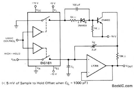
Switching transients are attenuated in sample-and-hold circuit using DG181 FET analog switch by adding neutralization derived from complementary signal coupled through upper switch of DG181. Charge transferred from second switch is then opposed to that from main channel. Circuit is controlled by input logic signal. With compensation, change in transferred charge is less than 5 picocoulombs for input signal range from -7.5 V to +7.5 V.- Analog Switches and Their Applications, Siliconix, Santa Clara, CA, 1976, p 7-61. (View)
View full Circuit Diagram | Comments | Reading(561)
14_KV_400_CPS_CRT_SUPPLY
Published:2009/7/20 21:26:00 Author:Jessie

Used to power special-purpose dark-trace tube. Triode in parallel with output provides voltage regulation to overcome effects of changing line voltage, improve output ripple, and improve output impedance characteristics.-NBS, Handbook Preferred Circuits Navy Aeronautical Electronic Equipment, Vol. 1, Electron Tube Circuits, 1963, p N14-1. (View)
View full Circuit Diagram | Comments | Reading(567)
Line_operated_15_kHz_inverter_with_120_volt_output
Published:2009/7/20 21:26:00 Author:Jessie

Line operated 15 kHz inverter with 120-volt output. This circuit can be used in ultrasonic applications and for high-frequency fluorescent lights. The output waveform is a 120-volt amplitude-modulated 15 kHz square wave (courtesy Motorola Semiconductor Products Inc.). (View)
View full Circuit Diagram | Comments | Reading(669)
7__10__15__20__25__35_watt_AF_power_amplifier_with_NPN_driver
Published:2009/7/20 21:26:00 Author:Jessie
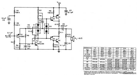
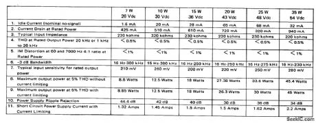
7-/10-/15-/20-/25-/35-watt AF power amplifier with NPN driver (courtesy Motorola Semiconductor Products Inc.). (View)
View full Circuit Diagram | Comments | Reading(1217)
BATTERY_VOLTAGE_REGULATOR
Published:2009/7/20 21:25:00 Author:Jessie

Used in battery-powered instruments to compensate for wide range of battery voltages. Converter serves to provide required variety of operating voltages and isolate equipment from sup ply. Will hold output within 0.5 v of 16 v for input range of 11.5 to 19 v.-C. D. Lind-say, Combined Battery Converter-Regulator Power Source, EEE, 14:3, p 61. (View)
View full Circuit Diagram | Comments | Reading(552)
ANALOG_SAMPLE_AND_HOLD
Published:2009/7/20 21:25:00 Author:Jessie

Uses AM685 comparator for continuous sampling of analog voltage at summing node formed by R1, and R2.Complementary logic outputs of comparator drive differential indicator formed by AM112 opamp. When error voltage at summing node is positive, comparator latches in high state and causes output opamp to integrate toward more negative voltage. When error voltage at latch time (determined by pulse input) is negative, integrator voltage ramps to more positive value. Circuit soon reaches equilibrium, at which out-put voltage is equal to -10 times value of sampled waveform. Article gives performance waveforms for sampling video pulses.-S. Den-'clinger, High-Speed Analog Sampler Uses Only Two IC's, EDN Magazine, May 20, 1977, p 128 and 130. (View)
View full Circuit Diagram | Comments | Reading(938)
Dual_voltage_transmitter_power_supply_with_800_volt_and_450_volt_taps
Published:2009/7/20 21:25:00 Author:Jessie

Dual-voltage transmitter power supply with 800-volt and 450-volt taps.This circuit Will handle a 100-watt transmitter,The 800-volt tap is rated at 175 mA intermittent duty with 1% ripple and 16% load rejection.The 450-volt tap is rated at 25 mA with 0.02% ripple. The voltage at V2 can be lowered to 375 volts by removing C3,The current rating of V2 can be Increased by selecting L3 with a higher current rating(courtesy General Electric Company). (View)
View full Circuit Diagram | Comments | Reading(626)
LOW_COST_VOLTAGE_REGULATOR
Published:2009/7/20 21:24:00 Author:Jessie
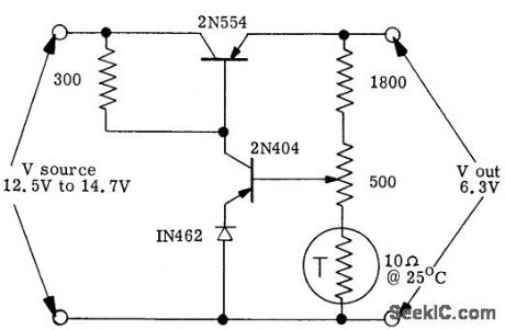
Costs 5 to 7 times less than toner regulator having same power rating. Can be set at precise voltage value required, whereas zener has 5 or 10% tolerance. Uses IN462 silicon diode for reference. Total cost (in quantity) is less than two dollars. Thermistor makes circuit perform from -55 to 71°C. Input voltage source is sea-water-activated batttery.-M. E. Gavin, Low Cost Transistor Voltage Regulator, EEE, 10:8, p 28-29.
(View)
View full Circuit Diagram | Comments | Reading(672)
BASIC_SERIES_PASS_REGULATOR
Published:2009/7/20 21:23:00 Author:Jessie
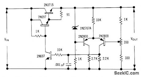
Output volt-age is regulated by 2N37l5 series-pass sill con power transistor having rise and fall limes below 0.5 microsec at 5 amp. Transistor has wide safe-area range, but circuit otherwise has no overload protection.-J. Takesuye and H. Weber, Silicon Power Transistors Provide New Solutions to Voltage Control Problems, Motorola Application Note AN-163, Aug. 1965. (View)
View full Circuit Diagram | Comments | Reading(881)
DIGITAL_SAMPLE_AND_HOLD
Published:2009/7/20 21:22:00 Author:Jessie
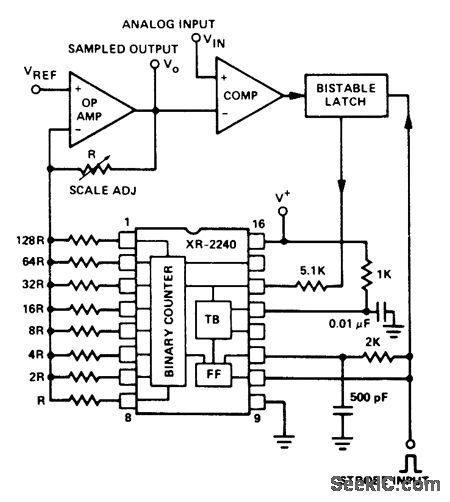
When strobe input is applied, RC low-pass network between reset and trigger inputs of Exar XR-2240 programmable timer/counter resets and then triggers timer, sets output of bistable latch to high state, and activates counter. Circuit generates staircase voltage at opamp output. When stair-case level reaches that of analog input to be sampled, comparator changes state, activates bistable latch, and stops count. Opamp output voltage level then corresponds to sampled analog input. Sample is held until next strobe signal. Minimum recycle time is about 6 ms. Sup-ply voltage can be 4-15V.- Timer Data Book, Exar Integrated Systems, Sunnyvale, CA, 1978, p11-18. (View)
View full Circuit Diagram | Comments | Reading(762)
BALANCED_INPUT_PENIODE_TWIN_IRIODE
Published:2009/7/20 21:58:00 Author:Jessie

Balanced input stage reduces effects of tube aging and heater voltage change. Plate load of 16,500 ohms on output pentode contributes to excellent frequency response. Neither reference tube nor comparison voltage divider are loaded. Gives outstanding over-all performance.-NBS, Handbook Preferred Circuits Navy Aeronautical Electronic Equipment.” 1, Electron Tube Circuits, 1963,p N2-4. (View)
View full Circuit Diagram | Comments | Reading(1948)
SAMPLE_HOLD_DISCRIMINATOR
Published:2009/7/20 21:57:00 Author:Jessie

Uses CMOS ICs and CMOS switches to minimize RF noise. Input from 10-kHz reference divider triggers CD4009 gate, and combination of diode and RC circuit produces sawtooth waveform having fast charge and slow discharge. Since input signal pulse may be too narrow, it is widened to 2μs by two-gate mono MVBR for controlling first CD4016 switch. Signal passed from first switch through 8007 opamp to second CD4016 switch is delayed by input of second switch to suppress unwanted spikes, so clean signal is fed through second 8007 opamp to T-notch filter having 10-kHz reference frequency for one leg and 20 kHz for other Ieg. Notch depth can be 60 dB. Filter drives VCO of frequency synthesizer through BCY59 emitter-follower transistor.-U. L. Rohde, Modem Design of Frequency Synthesizers, Ham Radio, July 1976, p10-23. (View)
View full Circuit Diagram | Comments | Reading(963)
COLOR_BURST_GATED_OSCILLATOR
Published:2009/7/20 21:57:00 Author:Jessie

For play-back of color tv recordings on magnetic tape, color burst is removed from composite video signal on tape, amplified by V1, and used to gate 3.58.Mc start-stop oscillator V2 to make this oscillator ring at burst frequency. Regenerated 3.58. Mc signal is am plified by V3 and fed to decoder for demodulating chroma information. -J. Roizen, Magnetic Recording of Color Television, Electronics, 33:1, p 76-79. (View)
View full Circuit Diagram | Comments | Reading(754)
5_digit_LED
Published:2009/7/20 21:56:00 Author:Jessie

5-digit LED (courtesy Motorola Semiconductor Products Inc.). (View)
View full Circuit Diagram | Comments | Reading(643)
TEMPERATURE_COMPENSATED_ZENER
Published:2009/7/20 21:56:00 Author:Jessie
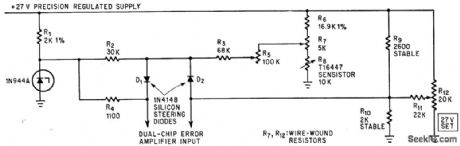
Reference voltage is compared to 27-v output by dual-chip transistor serving as error amplifier. Unique end-compensation circuit using sensistor generates voltage that rises with temperature.-C. H. Moulton, Light Pulse System Shrinks High-Voltage Protection Device, Electronics, 38:11, p 71-75. (View)
View full Circuit Diagram | Comments | Reading(716)
3_digit_ISUP2_SUPL_DPM_with_LED_interface
Published:2009/7/20 21:55:00 Author:Jessie

3-digit I2L DPM with LED interface (courtesy Analog Devices, Inc.). (View)
View full Circuit Diagram | Comments | Reading(487)
CHROMA_AMPLIFIER
Published:2009/7/20 21:55:00 Author:Jessie

Used in transistorized color tv to provide response slope opposite that of i-f amplifier. Automatic color control signal reduces voltage gain of first stage Q18. Color killer signal cuts off Q19 during monochrome opercation. -D, Bray, Solid State Makes Debut in Big-Screen Color Tv, Electronics, 39;8, p 99-105. (View)
View full Circuit Diagram | Comments | Reading(1333)
| Pages:943/2234 At 20941942943944945946947948949950951952953954955956957958959960Under 20 |
Circuit Categories
power supply circuit
Amplifier Circuit
Basic Circuit
LED and Light Circuit
Sensor Circuit
Signal Processing
Electrical Equipment Circuit
Control Circuit
Remote Control Circuit
A/D-D/A Converter Circuit
Audio Circuit
Measuring and Test Circuit
Communication Circuit
Computer-Related Circuit
555 Circuit
Automotive Circuit
Repairing Circuit