
Circuit Diagram
Index 953
_CONSTANT_SPEED_MOTOR_DRIVER
Published:2009/7/8 5:05:00 Author:May

When the torque load on the motor increases, its current increases. This current increase is sensed across RS, and positive feedback is applied to the noninverting terminal of the LH0101, thereby increasing the motor voltage to compen-sate for the increased torque load. With the proper amount of positive feedback, the motor-speed variation can be kept below 1% from no load to full load. (View)
View full Circuit Diagram | Comments | Reading(693)
Square_root_of_the_sum_of_the_squares_circuit
Published:2009/7/21 3:40:00 Author:Jessie

Square root of the sum of the squares circuit. This circuit performs vector computations (courtesy Analog Devices, Inc.). (View)
View full Circuit Diagram | Comments | Reading(959)
0_100°F_GIVES_0_1_kHz_OUTPUT
Published:2009/7/8 5:04:00 Author:May

Circuit provides direct temperature-to-frequ ency conver-sion at low cost for applications where digital output is desked. Temperature sensor is 1N4148 diode having -2.2 mV/°C temperature shift, controlling AD301 opamp in relaxation oscillator drcuit. Compensated 1N821 zener stabilizes against supply changes. Output network using 680 pF and 2.2K differentiates 400-ns reset edge of negative-going output ramp of opamp and drives single-transistor inverter to provide TTL output. Accuracy is within 0.3°F.-J. Williams, Designer's Guide to: Temperature Measurement, EDN Magazine, May 20, 1977, p 71-77.
(View)
View full Circuit Diagram | Comments | Reading(1453)
Multiplier_circuit_using_the_435_multiplier_divider_chip
Published:2009/7/21 3:37:00 Author:Jessie

Multiplier circuit using the 435 multiplier/divider chip (courtesy Analog Devices, Inc.). (View)
View full Circuit Diagram | Comments | Reading(609)
TACHLESS_MOTOR_SPEED_CONTROLLER
Published:2009/7/8 5:04:00 Author:May
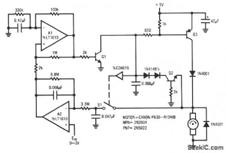
This circuit is particularly applicable to digitally-controlled systems in robotic and X-Y positioning applications. By functioning from the 5-V logic supply, it eliminates additional motor-drive supplies. The tachless feedback saves additional space and cost. The circuit senses the motor's back EMF to determine its speed. The difference between the speed and a set point is used to close a sampled loop around the motor. A1 generates a pulse train. When A1's output is high, Q1 is biased, and Q3 drives the motor's ungrounded terminal. When Al decreases, Q3 turns off and the motor's back EMF appears after the inductive flyback ceases. During this period, S1's input is turned on, and the 0.047-μF capacitor acquires the back EMF's value. A2 compares this value with the set point and the amplified difference (trace D) changes Al's duty cycle, controlling the motor speed. (View)
View full Circuit Diagram | Comments | Reading(0)
Square_rooter_using_the_433_multiplier_divider_chip
Published:2009/7/21 3:37:00 Author:Jessie

Square rooter using the 433 multiplier/divider chip (courtesy Analog Devices, Inc.). (View)
View full Circuit Diagram | Comments | Reading(606)
Square_rooter_circuit_using_the_434_multiplier_divider_chip
Published:2009/7/21 3:36:00 Author:Jessie

Square rooter circuit using the 434 multiplier/divider chip (courtesy Analog Devices, Inc.). (View)
View full Circuit Diagram | Comments | Reading(599)
Pulse_width_modulator_using_an_ECG955M_timer_oscillator_chip
Published:2009/7/21 3:35:00 Author:Jessie

Pulse width modulator using an ECG955M timer/oscillator chip. The flip-flop is connected in a monostable mode. The circuit is triggered with a continuous pulse train and the threshold voltage is modulated by the signal applied to control voltage pin 5. This has the effect of modulating the pulse width as control voltage varies (courtesy GTE Sylvania Incorporated). (View)
View full Circuit Diagram | Comments | Reading(783)
Two_quadrant_multiplication_with_the_AD7520_in_unipolar_binary_operation
Published:2009/7/21 3:34:00 Author:Jessie

Two-quadrant multiplication with the AD7520 in unipolar binary operation. The Intersil AD7520 is an 18-pin multiplying D/A converter. To adjust the zero offset connect all digital input to ground, and adjust the zero trimmer on the op amp for 0V ± 1 mV at VOUT. To adjust the gain connect all digital inputs of the AD7520 to VDD. Monitor VOUT for a -VREF ( 1 - 2-n ) reading, where n is equal to 10. To decrease VOUT connect a series resistor, 0 to 500 ohms, between the reference voltage and pin 15. To increase VOUT connect a series resistor, 0 to 500 ohms, in the VOUT1 amplifier feedback loop (courtesy Intersil, Inc.). (View)
View full Circuit Diagram | Comments | Reading(693)
RED_GREEN_LED_MONITOR
Published:2009/7/8 5:02:00 Author:May

Set points are adjusted by trimming resistor shunted across thermistor, to give onecolor when desired temperature has been reached and other color when temperature is low. Uses Monsanto MV5491 dual red/green LED, with 220 ohms in upper lead to +5 V supply and 100 ohms in Iower +5 V Iead because red and green LEDs in parallel back-to-back have different voltage rea quirements. LED drivers are SN75452 and SN75451.-K. Powell, Novel Indicator Circuit, Ham Radio, April1977, p 60-63. (View)
View full Circuit Diagram | Comments | Reading(676)
Color_TV_complete_video_amplifier_system_featuring_DC_contrast_and_brightness_DC_restorer_for_black_level_clamping_ganged_contrast_and_color_controls_and_ABL
Published:2009/7/21 7:05:00 Author:Jessie

Color TV complete video amplifier system featuring DC contrast and brightness, DC restorer for black-level clamping, ganged contrast and color controls and ABL (courtesy Motorola Semiconductor Products Inc.). (View)
View full Circuit Diagram | Comments | Reading(1111)
NEUTRALIZED_EMITTER_BOOSTS_H_F_GAIN
Published:2009/7/21 7:05:00 Author:Jessie

New operating mode increases h-f gain more thon 20 db, reduces interstage matching problems, improves selectivity and stability, and cuts cost. Based on neutralizing of emitter-circuit inductances with small variable capacitor from emitter to ground and r-f choke to provide d-c path from emitter to ground. Technique works best above 100 Mc.-Extend Transistor Frequency, Electronics, 34:44, p 25. (View)
View full Circuit Diagram | Comments | Reading(625)
1_W_AT_170_MC
Published:2009/7/21 7:04:00 Author:Jessie

Single L52 feeds 1 w to 50-ohm antenna through pi-L network. Power gain is 4 db and efficiency is 30% for class C operation.-Texas Instruments Inc., Solid.State Communications, McGraw-Hill, N.Y., 1966, p 323. (View)
View full Circuit Diagram | Comments | Reading(464)
CLOSED_LOOP_MOTOR_SPEED_CONTROL
Published:2009/7/8 5:01:00 Author:May
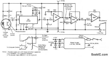
This electronic motor-speed control circuit is designed to operate in an electrically noisy environment.The circuit includes an optoelectronic pickup device, which is placed inside the motor housing to provide a speed feedback signal. The circuit automatically maintains the speed of the motor at the commanded value.
The pickup device contains an infrared LED and a phototransistor. The radiation from the diode is chopped into pulses by the motor fan blades, which are detected by the phototransistor. The train of pulses from the phototransistor is fed to a frequency-to-voltage converter, the output of which is a voltage proportional to the speed of the motor. This voltage is low-pass filtered, amplified, and compared with a manually-adjustable control voltage that represents the commanded speed.
The difference between the speed-measurement and speed-command signals is amplified and fed as a control voltage to an external power amplifier that drives the motor. A selector switch at the output of the final amplifier of this circuit also enables the operator to bypass the circuit and manually set the control voltage for the external amplifier. (View)
View full Circuit Diagram | Comments | Reading(799)
175_MC_F_M_MOBILE_AMPLIFIER
Published:2009/7/21 7:03:00 Author:Jessie

Overlay transistors operating directly from 13.5-v auto battery give 12 w from three stages and 35 w when output stage is added. Overall d-c to r-f efficiency of transmitter is about 60%.-D. J. Donahue and B. A. Jacoby, Putting the Overlay to Work at High Frequencies, Electronics, 38:17, p 78-81. (View)
View full Circuit Diagram | Comments | Reading(620)
TV_horizontal_processor_with_phase_detector_oscillator_and_predriver
Published:2009/7/21 6:23:00 Author:Jessie

TV horizontal processor with phase detector, oscillator, and predriver. Suited for all types of TV receivers, this circuit features internal shunt regulator, preset hold control capability, ±300-hertz pull-in, linear balanced phase detector, variable output duty cycle for driving tube or transistor, low thermal frequency drift, adjustable DO loop gain and positive flyback inputs (courtesy GTE Sylvania Incorporated). (View)
View full Circuit Diagram | Comments | Reading(2141)
ELECTRONICALLY_CONTROLLED_BANDWIDTH_
Published:2009/7/21 6:23:00 Author:Jessie
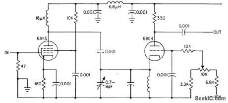
For search radar, potentiometer adjusts bias on 6BC4 tube of 30-Mc i-f preamp to vary bandwidth over range of 200 kc to 15 Mc.-Variable Bandwidth Preamplifier Electronically Varied Between 15 Mc and 200 Kc, Electronics, 35:2, p 102. (View)
View full Circuit Diagram | Comments | Reading(898)
VLF_PREAMP_WITH_AGC
Published:2009/7/21 6:22:00 Author:Jessie
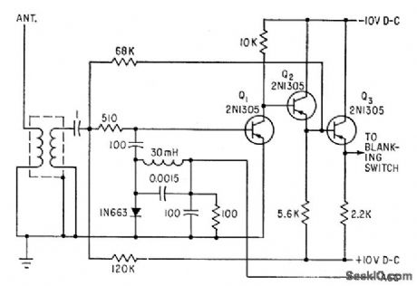
Fast-recovery computer diode acts as pure variable resistance shunting base of Q1 to ground, for full agc control without phase shift in output signal. In frequency range of 13 to 24 kc, phase shift is less than 0.25 microsec over 40-db input signal range.-J. D. Echols, Calibrating Frequency Standards with VLF Transmissions, Electronics, 35:17, p 60-63. (View)
View full Circuit Diagram | Comments | Reading(1004)
FOUR_THERMOCOUPLE_MULTIPLEXING
Published:2009/7/8 5:00:00 Author:May

Low power dissipation in DG306 analog switches means lower offset voltages added to thermo-couple voltages by silicon in contact with aluminum in switches. Thermocouples are switched differentially to instrumentation amplifier driving meter, in order to cancel thermal offsets due to switch.- Analog Switches and Their Applications, Siliconix, Santa Clara, CA, 1976, p 7-87. (View)
View full Circuit Diagram | Comments | Reading(481)
100__140__180_watt_linear_amplifier_for_16_to_30_MHz_136_volt_mobile_operation_
Published:2009/7/21 6:09:00 Author:Jessie

100-/140-/180-watt linear amplifier for 1.6 to 30 MHz 13.6-volt mobile operation (courtesy Motorola Semiconductor Products Inc.). (View)
View full Circuit Diagram | Comments | Reading(595)
| Pages:953/2234 At 20941942943944945946947948949950951952953954955956957958959960Under 20 |
Circuit Categories
power supply circuit
Amplifier Circuit
Basic Circuit
LED and Light Circuit
Sensor Circuit
Signal Processing
Electrical Equipment Circuit
Control Circuit
Remote Control Circuit
A/D-D/A Converter Circuit
Audio Circuit
Measuring and Test Circuit
Communication Circuit
Computer-Related Circuit
555 Circuit
Automotive Circuit
Repairing Circuit