
Circuit Diagram
Index 960
UNIVERSAL_MIXER_STAGE
Published:2009/7/8 4:30:00 Author:May

This circuit illustrates some possible buffer combinations. These include a differential input stage, a voltage follower as well as both noninverting and inverting stages. The allowable resistor ratios and recommended device types are also included. One restriction applies to this type of mixer network in which Rg is greater than 2.4 KΩ. This limits the worst case output current for each of the input buffers to less than 10 mA.
(View)
View full Circuit Diagram | Comments | Reading(923)
FOUR_CHANNEL_MIXER
Published:2009/7/8 4:28:00 Author:May

View full Circuit Diagram | Comments | Reading(0)
INPUT_BUFFERED_MIXER
Published:2009/7/8 4:27:00 Author:May
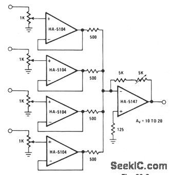
A high signal-to-noise ratio is important in stgnal construction and combination. The HA-5147 aids in lowering overall system noise and thereby raises system sensitivity. The signal combination circuit incorporates input buffering with several other features to form a relatively efficient mixer stage with a minimum of channel crosstalk. The potentiometer used for each channel allows for both variable input levels and a constant impedance for the driving source. The buffers serve mainly to prevent reverse crosstalk back through the resistor network. This buffering allows for the combination of varying strength signals without reverse contamination. The gain of the final stage is set at a minimum of 10 and can be adjusted to as much as 20.This allows a great amount of flexibility when combining a vast array of input signals. (View)
View full Circuit Diagram | Comments | Reading(1174)
Triac_static_motor_starting_switch_for_05_HP_115_volt_AC_single_phase_induction_motors
Published:2009/7/21 5:22:00 Author:Jessie

Triac static motor-starting switch for 0.5 HP 115-volt AC single-phase induction motors (courtesy Motorola Semiconductor Products Inc.). (View)
View full Circuit Diagram | Comments | Reading(1748)
Logic_to_inductive_load_interface_using_an_MOC3011_optically_coupled_triac_driver
Published:2009/7/21 5:21:00 Author:Jessie

Logic to inductive load interface using an MOC3011 optically coupled triac driver (courtesy Motorola Semiconductor Products Inc.). (View)
View full Circuit Diagram | Comments | Reading(7102)
SIMPLE_MIXER
Published:2009/7/8 4:26:00 Author:May

This mixer is built around a TL072 dual BiBET op anp with a JFET input stage,and can be powered from a single-ended 9-to 18-V power surry.The microphone input is capacitively coupled to the noninverting input of U1a.
Resistors R1 and R3 set the voltage gain at about 26 dB and serve as a negative feedback network for U1a.Capacitors C1 through C3 are dc-blocking capacitors.Most high-impedance microphones have outputs of a few mV.Often,a preamp stage just isn't enough,so the microphone signal is given a boost of about 20 db in the mixer.The noninverting input of U1b is biased to half the surry voltage by R6,R7,and C6.Rsistors R5 and R8 make up the negative-feedback network and set the voltage gain of U1b at unity.Capacitor C5 is for dc blocking at this input. (View)
View full Circuit Diagram | Comments | Reading(656)
1_W_EXCITER_FOR_7_AND_14_MHz
Published:2009/7/8 4:25:00 Author:May
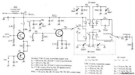
Developedfor use in simple solid-state VFO transmittercovering 40 and 20 meters for low-power operation Adequate drive can be provided by any 7-MHz VFO that develops 0.45 VRMS across 1000-ohm load. Circuit consists of olass A bufferl amplifier Q1 and keying switch Q2. Q3 is class C amplifier on 7 MHz (40m) and frequency doubler on 14 MHz (20m). Q1 is MPS6514. Q2 is 2N3906 or equivalent, Q3 is MPS-U31. All trans-former cores are Amidon T-50-2.—A. Weiss, QRP, CQ Nov. 1971, p 54-58 and 88. (View)
View full Circuit Diagram | Comments | Reading(807)
Color_TV_chroma_demodulator_with_level_shifted_output
Published:2009/7/21 5:21:00 Author:Jessie

Color TV chroma demodulator with level-shifted output. The ECG1099 is a 14-pin DiP with tab (courtesy GTE Sylvania Incorporated). (View)
View full Circuit Diagram | Comments | Reading(664)
SIGNAL_COMBINER
Published:2009/7/8 4:25:00 Author:May
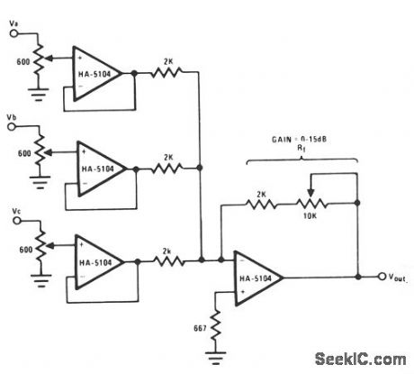
This circuit uses buffer stages to prevent channel crosstallk back through the mixer resistor network.The potentimeters used for each stage allow for convenient signal strength adjustment, while maintaining input impedance matching at the 600-Ω audio standard.The feedback resistor Rf will permit the output signal gain to be as high as 15 dB. (View)
View full Circuit Diagram | Comments | Reading(794)
DOOR_OPENER
Published:2009/7/8 4:24:00 Author:May

The door opener derives its power from a 9-V battery. A momentary-contact switch, S2, is provided in the event that manual opening and closing is required. Relay K1 is a 9-V type and relay K2 is a 117-Vac latching-type, which automatically latches with the first burst of current and opens on the second burst. The gate lead of the LASCR is not used;a light source triggers the LASCR unit into conduction, causing current to flow in the coil of the relay.That, in turn, causes K1's contacts to close,thereby energizing K2 (closing its contacts), and operating the garage door motor. (View)
View full Circuit Diagram | Comments | Reading(812)
Remote_control_receiver_for_TV
Published:2009/7/21 5:20:00 Author:Jessie

Remote control receiver for TV. Use ECG103 As for the relay drivers. Select the coils and transformers for the desired frequency. The ECG785 has a voltage gain of 129 dB at 40 kHz with the three internal amplifiers in cascade (courtesy GTE Sylvania Incorporated). (View)
View full Circuit Diagram | Comments | Reading(824)
_BUG_DETECTOR
Published:2009/7/8 4:23:00 Author:May

This rf detector can locate low-power transmitters (bugs) that are hidden from sight. It can sense the presence of a 1-mW transmitter at 20 feet, which is sensitive enough to detect the tiniest bug. As you bring the rf detector closer to the bug, more and more segments of its LED bar-graph display light, which aids in direction finding.
The front end has a two-stage wideband rf amplifier, and a forward-biased hot-carrier diode for a detector. After detection, the signal is filtered and fed to IC1, an LM3915N bar-graph driver having a logarithmic output. Each successive LED segment represents a 3-dB step. (View)
View full Circuit Diagram | Comments | Reading(2675)
Line_voltage_compensation_circuit_using_UJT_trigger_for_a_thyrister_gate
Published:2009/7/21 5:19:00 Author:Jessie
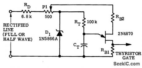
Line-voltage compensation circuit using UJT trigger for a thyrister gate (courtesy Motorola Semiconductor Products Inc.). (View)
View full Circuit Diagram | Comments | Reading(752)
T_ATTENUATOR_
Published:2009/7/8 4:22:00 Author:May

When inserted between stages of IF amplifier, circuit acts as three.section attenuator with dynamic range greater than 60 dB. Can be controlled by positive voltage from AVC system of receiver or manually with 100K pot. Use PIN diodes.-Super Circuits, 73 Magazine, Aug. 1975, p 140. (View)
View full Circuit Diagram | Comments | Reading(855)
SCR_model__railroading_control
Published:2009/7/21 5:19:00 Author:Jessie
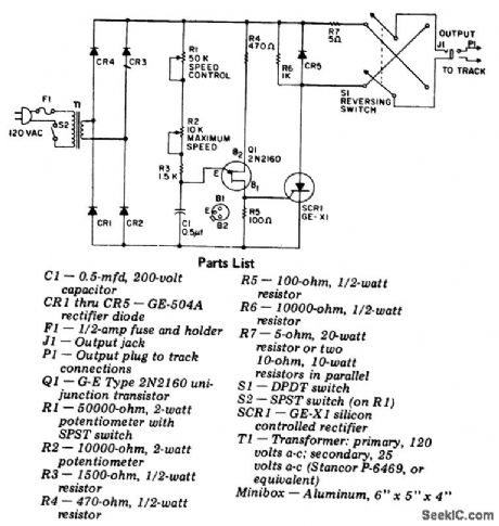
SCR model -railroading control. Bridge circuit CR1 through CR4 supplies pulsating DC to firing circuit Q1, R1 through R5 and C1, which phase controls SCR1. The SCR is in series with the train power and thereby controls the amount of current it receives (courtesy General Electric Company). (View)
View full Circuit Diagram | Comments | Reading(1310)
TRACK_AND_HOLD
Published:2009/7/8 4:22:00 Author:May

The 5-MHz track and hold shown here has a 400-kHz power bandwidth driving ±10 V. A buffered input follower drives the hold capacitor, C4, through Q1, a low resistance FET switch. The positive hold command is supplied by TTL logic, with Q3 level shifting to the switch driver, Q2. The output is buffered by A3. When the gate is driven to V- for hold, it pulls the charge out of the hold capacitor. A cornpensating charge is put into the hold capacitor through C3. The step into hold is made independent of the input level with R7, and adjusted to zero with R10.Since internal dissipation can be quite high when driving fast signals into a capacitive load, using a buffer in a power package is recommended. Raising the buffer quiescent current to 40 mA with R3 improves frequency response. (View)
View full Circuit Diagram | Comments | Reading(1120)
AIR_MOTION_DETECTOR
Published:2009/7/8 4:21:00 Author:May

When a current of air hits the piezo element, a small signal is generated and is fed through C1 and R1 to inverting input pin 2 of one section of the LM324. That causes output pin 1 to increase. Resistor R3 is used to adjust the sensitivity of the detector. The circuit can be set so high as to detect the vnvy of a hand or so low that blowing on the element as hard as you can will produce no output. Resistor R2 is used to adjust the level of the output voltage at pin 1.
The detector circuit can be used in various control applications. For example, an SCR can be used to control 117-Vac loads as shown. Also, an npn transistor, such as a TIP29, can be used to control loads as
(View)
View full Circuit Diagram | Comments | Reading(0)
TV_low_level_video_detector
Published:2009/7/21 5:18:00 Author:Jessie

TV low-level video detector. Typical voltage output is 7.5 volts peak to peak. The 14-pin DIP contains a double balanced detector circuit (courtesy GTE Sylvania Incorporated). (View)
View full Circuit Diagram | Comments | Reading(1277)
80_W_ON_2_METERS
Published:2009/7/8 4:20:00 Author:May

Single-stage design using two 2N6084 transistors combined with simple LC components can be tuned from 144 to 175 MHz. Typical input is 20W for 80-W output at 144 MHz. Article shows how to add 2N6083 driver stage that reduces input drive require-ment to 2,5 W. Power gain at 144 MHz is 6 dB. Article covers construction and adjustment.—J. Hatchett, A Solid 80 Watts fol Two Meters, Ham Radio, Dec. 1973, p 6-12. (View)
View full Circuit Diagram | Comments | Reading(3306)
Color_TV_chroma_amplifier_demodulator_using_an_ECG791_16_pin_DIP
Published:2009/7/21 5:17:00 Author:Jessie

Color TV chroma amplifier/demodulator using an ECG791 16-pin DIP. The circuit features shotl-circuit protection, ACC, and color killer. Typical sensitivity of chroma input is 10 mV RMS with a 50 mV sensitivity for amplifier 2 at pin 4 (courtesy GTE Sylvania Incorporated). (View)
View full Circuit Diagram | Comments | Reading(1141)
| Pages:960/2234 At 20941942943944945946947948949950951952953954955956957958959960Under 20 |
Circuit Categories
power supply circuit
Amplifier Circuit
Basic Circuit
LED and Light Circuit
Sensor Circuit
Signal Processing
Electrical Equipment Circuit
Control Circuit
Remote Control Circuit
A/D-D/A Converter Circuit
Audio Circuit
Measuring and Test Circuit
Communication Circuit
Computer-Related Circuit
555 Circuit
Automotive Circuit
Repairing Circuit