About SeekIC | Services | Payment | Advertisements service | Contact Us | Links
© 2008-2012 SeekIC.com Corp.All Rights Reserved.

Published:2009/7/20 22:15:00 Author:Jessie

Use of 2N4393 JFET at input of opamp gives simple high-performance circuit having low leakage,Offset is easily adjusted with 1K pot.- FET Databook, National Semiconductor, Santa Clara,CA,1977,p6-26-6-36. (View)
View full Circuit Diagram | Comments | Reading(0)
Published:2009/7/20 22:15:00 Author:Jessie

27 MHz mixerfor CB operation using a TIS148 dual-gate MOSFET (courtesy Texas Instruments Incorporated). (View)
View full Circuit Diagram | Comments | Reading(552)
Published:2009/7/20 22:14:00 Author:Jessie

Three-stage class A amplifer provides output of 2 w. Feedback from emitter of Q9 to base of Q7 provides over-all d-c stability.-D. Bray, Solid State Makes Debut in Big-Screen Color Tv, Electronics, 39:8, p 99-105. (View)
View full Circuit Diagram | Comments | Reading(711)
Published:2009/7/20 22:13:00 Author:Jessie

Provides burst gating pulses for operating balanced-diode pate used in studio switching of color tv programs.-J. O. Schroeder, Holding Video levels While Switching Studios, Electronics, 32:22, p 96-98. (View)
View full Circuit Diagram | Comments | Reading(704)
Published:2009/7/20 22:13:00 Author:Jessie

Power function generator developing sine waves,triangular waves and square waves. Operating frequency is 2 hertz to 20 kilohertz. VO is up to ±25 volts (50 volts peak to peak) across loads as small as 10 ohms, which produces a maximum of 2.5 amperes of output current. All capacitor working voltage ratings should be 50 volts DC. All resistors should be the half-watt type unless otherwise specified. Keep the lead at pin 2 of the op amp less than 2 inches or oscillations will result. Full power output is only obtainable up to about 5 kilohertz due to the op amp (courtesy Intersil, Inc.). (View)
View full Circuit Diagram | Comments | Reading(1468)
Published:2009/7/20 22:13:00 Author:Jessie

3-digit I2L DPM with LED/CPU interface(courtesy Analog Devices, Inc.). (View)
View full Circuit Diagram | Comments | Reading(665)
Published:2009/7/20 22:13:00 Author:Jessie

Single demodulator in Japanese 7-inch color tv recovers the three difference signals in sequence by impressing color signal with load subcarrier that is advanced 120°in phase for each line. -Y. Sugihara, H. Ito and A. Horaguchi, From Japan a Startling New Color TV Set, Electronics, 38:11, p 81-94. (View)
View full Circuit Diagram | Comments | Reading(857)
Published:2009/7/20 22:12:00 Author:Jessie

27 MHz autodyne tuner using a 3N225 dual-gate MOSFET (courtesy Texas Instruments Incorporated). (View)
View full Circuit Diagram | Comments | Reading(841)
Published:2009/7/20 22:12:00 Author:Jessie
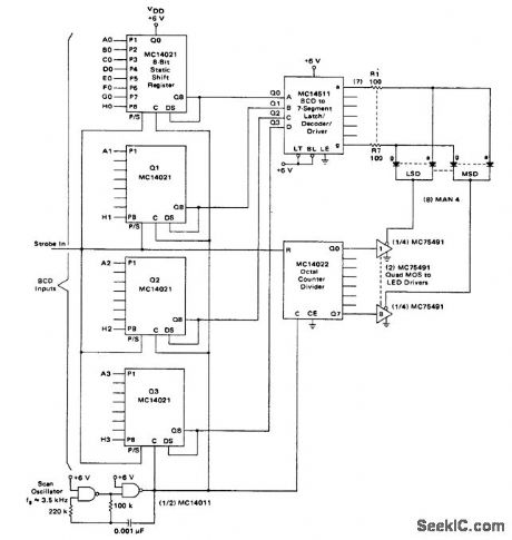
8-digit multiplexed LED (courtesy Motorola Semiconductor Products Inc.). (View)
View full Circuit Diagram | Comments | Reading(1284)
Published:2009/7/20 21:41:00 Author:Jessie
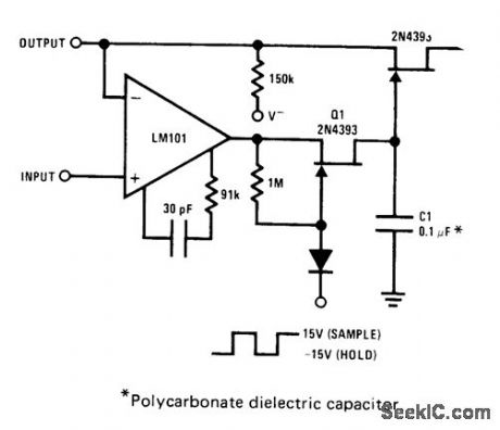
JFETs provide complete buffering to sample-and-hold capacitor C1. During sample, al is turned on to provide charging path. During hold, Q1 and Q2 are turned off so discharge paths through transistors for C1 are each less than 100 pA.Q2 also serves as buffer for opamp so feedback and out-put current are supplied only from opamp source.- FET Databook, National Semiconductor, Santa Clara, CA, 1977, p 6-26-6-36. (View)
View full Circuit Diagram | Comments | Reading(0)
Published:2009/7/20 21:40:00 Author:Jessie

Meter indicates output signal when input is present and stores input in C1 when samples witch is open. Opamp is connected as unity-gain voltage follower. Charge on C1 will be drained within a few minutes by opamp shown. Charge can be held longer by changing to FET-input opamp or by opening both battery circuits with alternative DPDT switch SW2.Developed for classroom demonstrations.-F. M. Mims, Integrated Circuit Projects, Vol. 4, Radio Shack, Fort Worth, TX, 1977, 2nd Ed., p 61-69. (View)
View full Circuit Diagram | Comments | Reading(693)
Published:2009/7/20 21:39:00 Author:Jessie

Arrangement gives high gain, approaching 10,000, along with more ripple reduction than is generally required.-NBS, Hand-book Preferred Circuits Navy Aeronautical Electronic Equipment, Vol. 1, Electron Tube Circuits, 1963, p N2-4. (View)
View full Circuit Diagram | Comments | Reading(685)
Published:2009/7/20 21:37:00 Author:Jessie
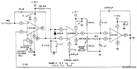
CA3160 opamp provides high input impedance and input voltage range of 0-10V. CA3080A functions as strobed current source for CA3140 output integrator and storage capacitor. Pulse droop during hold interval can be reduced to zero by adjusting 100K pot.- Linear Integrated Circuits and MOS/FET's, RCA Solid State Division, Somerville, NJ, 1977, p 271-272. (View)
View full Circuit Diagram | Comments | Reading(1496)
Published:2009/7/20 21:37:00 Author:Jessie

Has self-contained reference voltage, and does not load reference tube. Is theoretically capable of highest possible gain obtainable with single-envelope d-c amplifiers.-NBS, Handbook Preferred Circuits Navy Aeronautical Electronic Equipment, Vol. 1, Electron Tube Circuits, 1963, p N2-3. (View)
View full Circuit Diagram | Comments | Reading(679)
Published:2009/7/20 21:36:00 Author:Jessie

Permits wider supply voltage range and better operation thon arrangements using self-contained reference.-NBS, Hand. book Preferred Circuits Navy arrangements Electronic Equipment, Vol. 1, Electron Tube Circuits, 1963, p N2-4. (View)
View full Circuit Diagram | Comments | Reading(758)
Published:2009/7/20 21:36:00 Author:Jessie
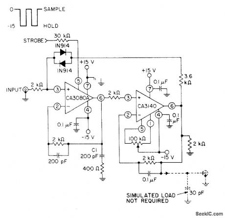
CA3140 bipolar M0S opamp serves as readout amplifier for storage capacitor C1 which is charged by CA3080A variable opamp serving as input buffer and low-feedthrough transmission switch. CA3140 also provides offset nulling.- Circuit Ideas for RCA Linear ICs, RCA Solid State Division, Somerville, NJ, 1977, p 17. (View)
View full Circuit Diagram | Comments | Reading(0)
Published:2009/7/20 21:35:00 Author:Jessie


15-/20-/25-watt AF power amplifier with Darlington outputs (courtesy Motorola Semiconductor Products Inc.). (View)
View full Circuit Diagram | Comments | Reading(3293)
Published:2009/7/20 21:35:00 Author:Jessie

Multi output low-voltage power supply for TEL and CMOS (courtesy Motorola Semiconductor Products Inc.). (View)
View full Circuit Diagram | Comments | Reading(1818)
Published:2009/7/20 21:35:00 Author:Jessie

Reference lube is in cathode circuit of 6AK5, and plate load of pentode is high (1 meg), resulting in poor frequency response.-NBS, Handbook Preferred Circuits Navy Aeronautical Electronic Equipment, Vol. 1, Electron Tube Circuits, 1963, p N2-2. (View)
View full Circuit Diagram | Comments | Reading(865)
Published:2009/7/20 21:35:00 Author:Jessie
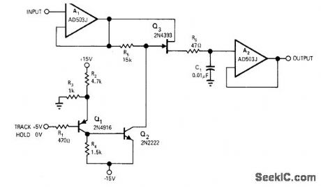
Developed for tracking ±10 V AF input signal when control input is +5 V. When control drops to 0 V, series FETQ3 opens and input voltage at that time is stored on C1 for transfer to output through high impedance opamp A2.-R. S. Burwen, Track-and-Hold Amplifier, EDNIEEE Magazine, Sept.1, 1971, p 43. (View)
View full Circuit Diagram | Comments | Reading(715)
| Pages:942/2234 At 20941942943944945946947948949950951952953954955956957958959960Under 20 |
Response in 12 hours
© 2008-2012 SeekIC.com Corp.All Rights Reserved.