
Circuit Diagram
Index 959
DIFFERENTIAL-TO_SINGLE_ENDED_VOLTAGE_AMPLIFIER
Published:2009/7/8 4:38:00 Author:May
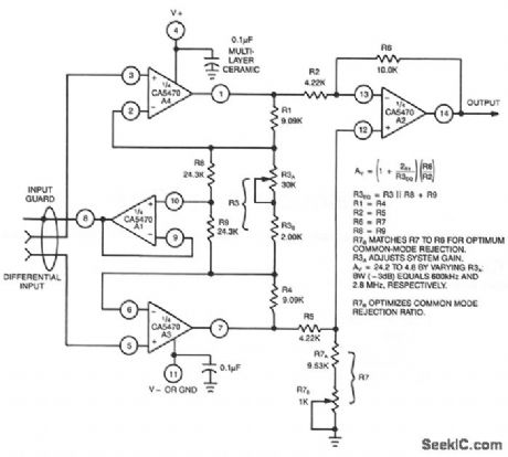
This circuit uses a CA5470 quad microprocessor BiMOS-E op amp. Amplifiers A1 and A2 are employed as a cross-coupled differential input and differential output preamp stage and A3 provides input guard-banding. Amplifier A4 converts the differential outputs of A and A2 to a single-ended output. (View)
View full Circuit Diagram | Comments | Reading(929)
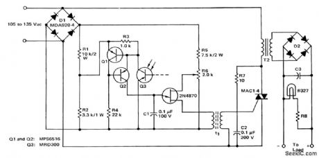
MODULATION_MONITOR
Published:2009/7/8 4:37:00 Author:May

Switching diodes are used to fire the neon lamps when negative-peak modulation hits 50, 60, and 100%. To use the circuit, keep an eye on the lamps. You should attempt to keep the 50% lamp firing all the time, the 60% lamp should be on as much as possible, but try to prevent the 100% lamp from lighting. (View)
View full Circuit Diagram | Comments | Reading(0)
Complete_TV_vertical_circuit_with_AFC_for_90_decree_20_inch_receivers
Published:2009/7/21 5:00:00 Author:Jessie

Complete TV vertical circuit with AFC for 90-decree 20-inch receivers (courtesy GTE Sylvania Incorporated). (View)
View full Circuit Diagram | Comments | Reading(760)
65_KV_TWIN_TRIODE_A_F_OSCILLATOR_CRT_SUPPLY
Published:2009/7/21 5:00:00 Author:Jessie

Oscillator develops square wove because of saturable square-loop core materical of transformer. Diodes eliminate extra load placed on oscillator by high-vacuum rectifier tube filaments. –NBS, Handbook Preferred Circuits Navy Aeronautical Electronic Equipment, Vol. 1, Electron Tube Circuits, 1963, p N14-5. (View)
View full Circuit Diagram | Comments | Reading(679)
BF_MODULATOR
Published:2009/7/8 4:36:00 Author:May
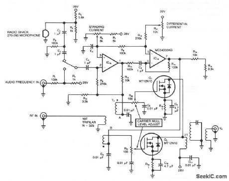
Because power MOSFETs offer high power gain at both audio and radio frequencies, they are useful in many areas of radio-circuit design. For rf applications, a MOSFET's large safe operating area, VDS vs ID, protects it against damage from reflected rf energy. As a modulator, a MOSFET's transfer linearity aids fidelity. In the suppressed-carrier modulator, an rf signal is applied to the primary of transformer T1, whose secondaries provide equal-amplitude, opposite-phase rf drive signals to output FETs Q1 and Q2.Output V0 is zero when no audio-frequency signals are present, because the opposite-phase rf signals from Q1 and Q2 cancel. When audio-frequency signals appear at nodes A and B, you obtain a modulated rf output (V0). Source resistors R18 and R19 improve the dc stability and low-frequency gain. A phase inverter, based on the dual op amp IC1A and IC1B, generates the out-of-phase, equal-amplitude, audio-frequency modulation signals. (View)
View full Circuit Diagram | Comments | Reading(831)
QMULTIPLIER_
Published:2009/7/8 4:34:00 Author:May

Transistorized Q multiplier can be connected to plate of mixer in receiver having IF in range of 1400-1500 kHz. Iron-core coil should have high a. Setting of pot depends on transistor used, which could also be HE-3 or 2N1742.-Q&A, 73 Magazine, April 1977,p 165. (View)
View full Circuit Diagram | Comments | Reading(1211)
TV_video_IF_amplifier_and_detector_using_two_8_pin_DIPs
Published:2009/7/21 4:58:00 Author:Jessie

TV video IF amplifier and detector using two 8-pin DIPs.Powergain is as fallows∶60 dB at 45 MHz(pin 3 open), 56 dB at 58 MHz(pin 3 open),61 dB at 45 MHz(pin 3 bypassed),and 59 dB at 58 MHz(pin 3 bypassed).AGC range is 80 dB from DC to 45 MHz,C4 should be 0.002 μF at 45 MHz(courtesy GTE Sylvania Incorporated). (View)
View full Circuit Diagram | Comments | Reading(676)
SAW_SOCILLATOR_MODULATOR
Published:2009/7/8 4:34:00 Author:May
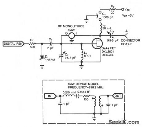
Adding a diode, a resistor, and a capacitor to the SAW (surface-acoustic-wave) oscillator allows you to use the oscillator in FSK (frequency-shift-keying) applications. D1, R1, and C1 form a simple diode switch in which D1 shunts C1 to ground. When the digital FSK input to R1 is low, D1 is off, and the small junction capacitance of D1 couples C1 to ground. A high FSK signal causes current to flow through R1 and D1.D1's dynamic impedance is small when it is in forward conduction. Therefore, C1 sees a lower impedance path to ground. Thus, the FSK input effectively switches C1 in and out of the oscillator's circuit.
When C1 is in the circuit-digital FSK is high-it pulls the frequency of the circuit slightly lower because of the additional phase shift C1 introduces at the GaGs FET gate terminal (available from: Dexcel, Div. of Gould, Santa Clara, CA). The SAW device (available from: RF Monolithics, Dallas, TX) restricts the amount of frequency shifting-usually less than 20 ppm for a high-Q SAW device.
The oscillator shown produces a center frequency of 896.2 MHz with an FSK deviation of 17 kHz when you drive the FSK input with a 0 to 5 V signal. The frequency also depends on L1 and C2.
(View)
View full Circuit Diagram | Comments | Reading(671)
OSCILLATOR_TYPE_SUPPLY_
Published:2009/7/21 4:57:00 Author:Jessie
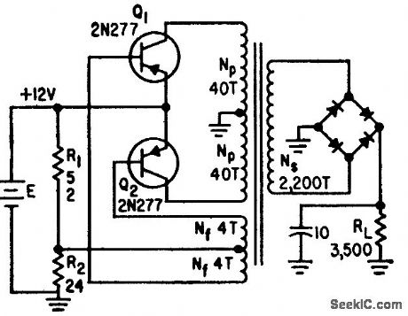
Article gives basic design equations for d-c power supply using power transistors. Efficiency is up to 90%. D-c output voltage is 590 V for 3,500-ohm load. –T. Hamm, Jr., Equations for Designing Transistor Power Supplies, Electronics, 32:43, p 122-124. (View)
View full Circuit Diagram | Comments | Reading(899)
Remote_control_for_lamp_or_appliance_using_a_reed_switch_and_coil
Published:2009/7/21 4:57:00 Author:Jessie
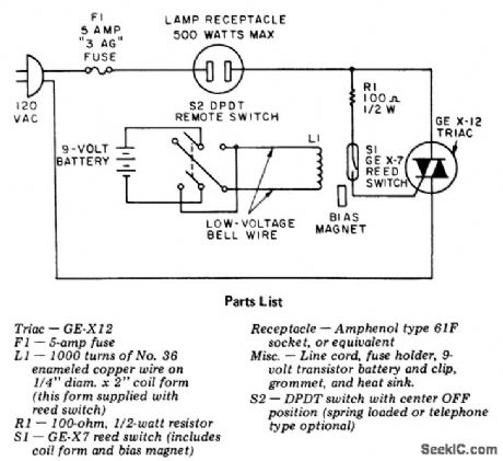
Remote control for lamp or appliance using a reed switch and coil. The circuit will handle up to 500 watts (courtesy General Electric Company). (View)
View full Circuit Diagram | Comments | Reading(663)
RECEIVER_CHECKER
Published:2009/7/21 4:55:00 Author:Jessie

Single-transistor 28-MHz crystal oscillator and carefully designed attenuator network serve to generate signal of about 1μA for checking performance of amateur radio receiver, Can be used on any band down to 6 meters by appropriate choice of crystal and LC circuit components. Coil is CTC LS5 form having 15 turns No. 22 enamel and 2-turn link.-Is It the Band or My Receiver?, 73 Magazine, Oct. 1976, p 132-133. (View)
View full Circuit Diagram | Comments | Reading(687)
Triac_control_circuit_employing_an_ECG776_zero_voltage_switch_with_current_boost_utilizing_an_AC_supply
Published:2009/7/21 4:54:00 Author:Jessie

Triac control circuit employing an ECG776 zero voltage switch with current boost utilizing an AC supply. The circuit is for applications requiring gate currents greater than 50 mA. Select the triac from the ECG5600 series for the particular application (courtesy GTE Sylvania Incorporated). (View)
View full Circuit Diagram | Comments | Reading(2583)
SIGNAL_TRACK_AND_HOLD
Published:2009/7/8 4:34:00 Author:May
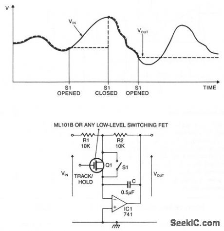
When the switch is closed or the FET is conducting, the circuit behaves as an inverting amplifier with a gain of R2/R1. Since as the inverting terminal of the op amp is a virtual ground, the capacitor is kept charged to the output voltage by the op amp. When the switch is opened and the FET is nonconducting, the voltage at the output is held constant by the capacitor, the current demands of the next stage are met by the op amp. The value of C should be chosen so that its impedance at the operating frequency is large compared to R1 and R2. (View)
View full Circuit Diagram | Comments | Reading(617)
MODULATOR
Published:2009/7/8 4:33:00 Author:May

Because the transconductance of an operational transconductance amplifier is directly proportional to IABC, the amplification of a signal can be controlled easily. The output current is the product from transcon-ductance X input voltage. The circuit is effective up to approximately 200 kHz. Modulation of 99% is easy to achieve. (View)
View full Circuit Diagram | Comments | Reading(837)
100_kHz_CAUBFIATOR
Published:2009/7/21 4:54:00 Author:Jessie

Simple crystal-controlled single-transistor oscillator can be used to calibrate amateur radio transceiver. Output should be connected to antenna input side of receiver, not to antenna terminal normally used.-Novice Q & A, 73Magazine, March 1977, p 187. (View)
View full Circuit Diagram | Comments | Reading(695)
0_1200_V_REGULATED_SUPPLY_FOR_RHOTOMULTIPLIER
Published:2009/7/21 4:54:00 Author:Jessie
Silicon diodes in R-C filter network gives 0.2% regulation over entire d-c output range, with temperature cosfficient only 0.1% of output voltage per deg C, for photomultiplier stage in airborne equipment. –J. G. Peddie, Network Filters Stabilize d-c Supply Over Wide Range, Electronics, 37:18, p 83. (View)
View full Circuit Diagram | Comments | Reading(634)
107_MHz_IF_for_FM
Published:2009/7/8 4:32:00 Author:May

Motorola dual MC1355 limiting gain blocks are used with two TRW fivepole linear phase filters and external ratio detector to give complete high-performance IF amplifier for FM receiver. MPS-H04 discrete transistor is used after first filter block to reduce noise figure for overall system. Input and output impedances are 235 ohms.-''lntegrated Circuit IF Amplifiers for AM/FM and FM Radios, Motorola, Phoenix, AZ, 1975, AN-543A, p 4. (View)
View full Circuit Diagram | Comments | Reading(1470)
POSITIVE_AND_NEGATIVE_VOLTAGE_REFERENCE_TRACKER
Published:2009/7/8 4:31:00 Author:May
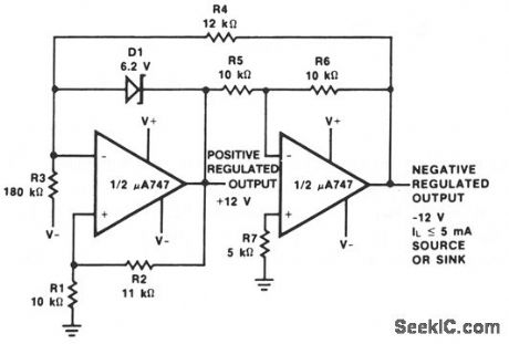
This reference uses an op amp to derive a negative output voltage that tracks with the positive reference voltage. A μA747 dual op amp, or any similar device such as an LM1458 or two pA741 devices, can be used.Positive Output = VD1×(R1+R2)/R2Negative Output =-Positive Output × R6/65 (View)
View full Circuit Diagram | Comments | Reading(1303)
RMS_regulator_for_a_DC_power_supply_using_a_triac_phototransistor_and_UJT
Published:2009/7/21 4:51:00 Author:Jessie
RMS regulator for a DC power supply using a triac, phototransistor and UJT (courtesy Motorola Semiconductor Products Inc.). (View)
View full Circuit Diagram | Comments | Reading(1799)
RF_MODULATOR
Published:2009/7/8 4:31:00 Author:May
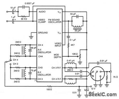
Two IC rf modulators convert a suitable baseband video and audio signal up to a low VHF modulated carrier-Channel 2 through 6 in the U.S., and 1 through 3 in Japan-the LM1889 and the LM2889. Both ICs are identical regarding the rf modulation function, including pin outs, and can provide either of two rf carriers with dc switch selection of the desired carrier frequency. The LM1889 includes a crystal-controlled chroma subcarrier oscillator and balanced modulator for encoding R through Y or U and V color difference signals. A sound intercarrier frequency lc oscillator is modulated using an external vatactor diode. The LM2889 replaces the chroma subcarrier function of the LM1889 with a video dc restoration clamp and an internal frequency-modulated sound intercarrier oscillator.
(View)
View full Circuit Diagram | Comments | Reading(5108)
| Pages:959/2234 At 20941942943944945946947948949950951952953954955956957958959960Under 20 |
Circuit Categories
power supply circuit
Amplifier Circuit
Basic Circuit
LED and Light Circuit
Sensor Circuit
Signal Processing
Electrical Equipment Circuit
Control Circuit
Remote Control Circuit
A/D-D/A Converter Circuit
Audio Circuit
Measuring and Test Circuit
Communication Circuit
Computer-Related Circuit
555 Circuit
Automotive Circuit
Repairing Circuit