
Circuit Diagram
Index 929
REMOTE_CONTROL_FOR_SERVO_POSITION
Published:2009/7/21 1:29:00 Author:Jessie
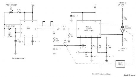
Setting of pot R, in circuit of remotely located 555 timer determines position of 11.5-ohm servomotor by feeding appropriate square-wave pulses over wire line to servoamplifier. - Signetics Analog Data Manual, Signetics, Sunnyvale, CA, 1977, p 727-728. (View)
View full Circuit Diagram | Comments | Reading(1487)
400_Hz_AMPLIFIER
Published:2009/7/21 1:32:00 Author:Jessie
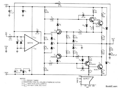
Developed to increase output power of digital-to-synchro converter systems while providing stable and accurate output and overall gain even with reactive loads, at Includes overload protection. Delivers 95 VRMS 400 Hz continuously into 500-ohm load. Power bandwidth is about 20 kHz. Foldback current limiting drops short-circuit current to 200mA when load exceeds 300 mA.-F. H. Catter-molen and J. A. Pieterse, Digital/Synchro Amplifier Features Overload Protection, EDN Magazine, Nov. 5, 1977, p 107-108. (View)
View full Circuit Diagram | Comments | Reading(2532)
Sensitive photoelectric receiver circuit diagram
Published:2011/8/3 2:40:00 Author:Rebekka | Keyword: Sensitive photoelectric receiver
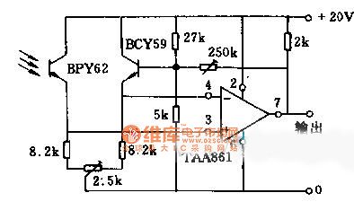
The circuit phototransistor BPY62 isparallel with temperature compensation transistors BCY59. It constitutes a differential amplifier. Two tubes require the same type of product which are matching pairs. The sensitivity can be adjusted by 250KΩ potentiometer. The adjustment margin is 1:5 times. When the average output voltage is 10V, its corresponding light intensity is about 200lx. The adjustment of2.5KΩ potentiometer can calibrate the balance voltage between symmetry and DC. (View)
View full Circuit Diagram | Comments | Reading(1405)
Analog_multiplier_using_an_ECG947_dual_operational_amplifier
Published:2009/7/21 2:03:00 Author:Jessie

Analog multiplier using an ECG947 dual operational amplifier. The ECG947 is short-circuit protected and requires no external components for frequency compensation (courtesy GTE Sylvania Incorporated). (View)
View full Circuit Diagram | Comments | Reading(645)
CENTER_TAPPED_TRANSFORMER_AUDIO_OSCILLATOR
Published:2009/7/21 2:03:00 Author:Jessie

The oscillator circuit uses a center-tapped transistor output transformer to serve as a load for the collector of Q1, supply a feedback signal for the base, and serve as the output winding for driving the speaker. R1 supplies dc bias and C1 completes the ac path from the transformer to Q1's base. You can play around with the values of C1 and R1 to change the oscillator's output level and tone, but don't reduce R1's value too much or the transistor will draw excessive collector current. (View)
View full Circuit Diagram | Comments | Reading(3324)
Difference_of_squares_circuit
Published:2009/7/21 2:04:00 Author:Jessie

Difference-of-squares circuit. This circuit computes the difference of the squares of two input signals. It is useful in vector computations and in weighing the difference of two magnitudes to emphasize the greater nonlinearity. It can also be used to determine absolute value if A is the input, B is connected to EO through a diode and both Z terminals are grounded (courtesy Analog Devices, Inc.). (View)
View full Circuit Diagram | Comments | Reading(544)
SIX_RANGE_RF
Published:2009/7/21 2:04:00 Author:Jessie

Covers from 100 kHz to about 75 MHz in six bands, for checking low-frequency IF circuits on up to VHF circuits (using harmonics up to 220 MHz). Omission of frequency read-out dial scale simplifies design without affecting usefulness for troubleshooting. FETs can be HEP-802 or MPF102, and output transistor is 2N3866 or 2N706, First FET is Hartley oscillator lightly coupled through 5-pF capacitor to FET source-follower isolation stage. Last stage boosts signal level up to about 1 V on most bands. Tuning capacitor is broadcast-band type having 300-pF AM section and 25-pF FM section. Set of six coils can be purchased as Conar CO-69 through CO-74 from National Radio Institute or can be wound as suggested in article to give high-end band limits of 0.57, 1.4, 4.5, 17, 39, and 75-80 MHz. For portable use, 12-V battery pack or 9-V transistor radio battery can be used to give constant 9-V supply.-Brew Up a Signal Generator, 73Magazine, Jan. 1978, p 50-52. (View)
View full Circuit Diagram | Comments | Reading(786)
SCR_phase_control_circuit_with_a_PUT
Published:2009/7/21 2:04:00 Author:Jessie
SCR phase control circuit with a PUT. Relaxation oscillator Q2 provides conduction control of Q1 from 1 ms to 7.8 ms (courtesy Motorola Semiconductor Products Inc). (View)
View full Circuit Diagram | Comments | Reading(961)
30_Hz_TO_100_kHz
Published:2009/7/21 2:06:00 Author:Jessie

Wien-bridge sine-wave oscillator using two RCA CA3140 opamps covers frequency range with less than 0.5% total harmonic distortion. Adjust 10K pot for best output waveform. Maximum output into 600-ohm load is about 1 VRMS. Opamps are direct replacements for 741 but have higher input impedance and better slew rate.-C. Hall, New Op Amp Challenges the 741, Ham Radio, Jan. 1978, p 76-78. (View)
View full Circuit Diagram | Comments | Reading(685)
CRYSTAL_CONTROLLED_AUDIO_GENERATOR
Published:2009/7/21 2:06:00 Author:Jessie
In this circuit, two signals from crystal oscillators operating at nearly the same frequency are mixed in Q2 and the audio difference frequency is used. C3 is a small air padder capacitor of 3 to 40 pF and can be fitted with a dial that is calibrated in the audio frequency producedi C2 is used for an initial calibration of the fixed oscillator to exactly 10.000 MHz. (View)
View full Circuit Diagram | Comments | Reading(780)
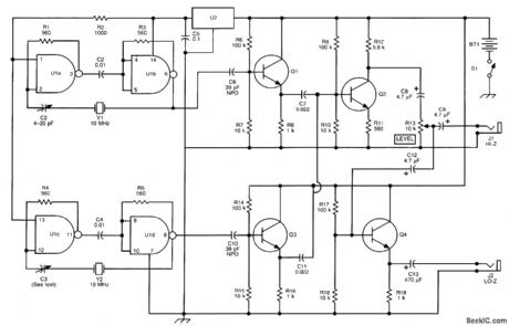
TC9149P/TC9150F (Video recorder and TV set) infrared remote control receiving circuit
Published:2011/7/27 19:08:00 Author:TaoXi | Keyword: Video recorder, TV set, infrared, remote control, receiving circuit
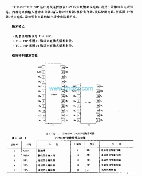
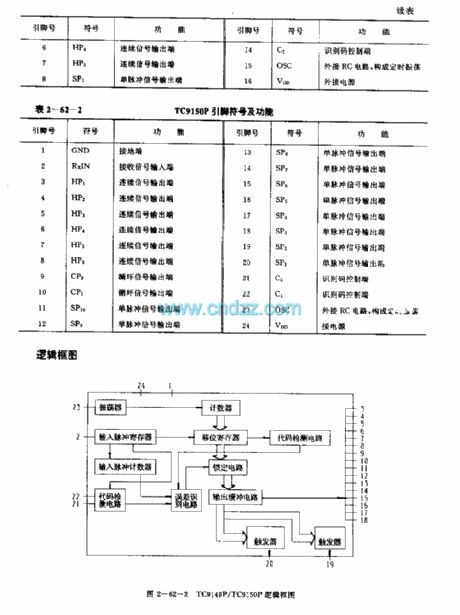


The TC9149P/TC9150F is designed as the infrared remote control receiving CMOS large-scale circuit that can be used in the video recorder and TV set applications. The internal circuit is composed of the input pulse register, the input pulse counter, the shift register, the code detection circuit, the oscillator, the counter, the locking circuit, the error identification circuit and the output buffer circuit.
Features
The matching model is TC9148P.The TC9149P uses the 16-pin dual-row DIP plastic package.The TC9150P uses the 24-pin dual-row DIP plastic package.
Function declaration
The oscillation frequency of the oscillator is decided by the external resistance and capacitance.The signal adds to the signal receiving input port pin-2 after it is amplified and detected by the circuit.
(View)
View full Circuit Diagram | Comments | Reading(1998)
TA7657P (electronic toys) radio remote control receiving circuit
Published:2011/7/27 3:59:00 Author:TaoXi | Keyword: electronic toys, radio, remote control, receiving circuit
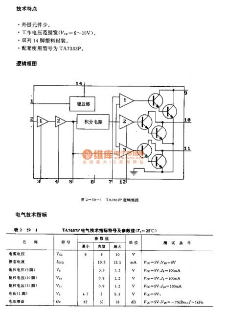

The TA7657P is designed as one kind of radio remote control receiving circuit that can be used in the electronic toys. The internal circuit is composed of the amplifier, the voltage stabilizer, the integral circuit, the comparator and the driver.
Features
Little external components.Wide operating voltage range (Vcc=6-10V).Dual-row 14-pin plastic package.The matching model is TA7333P.
(View)
View full Circuit Diagram | Comments | Reading(2249)
PHOTODIODE_SOURCE_FOLLOWER
Published:2009/7/8 22:58:00 Author:May
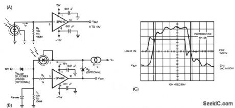
A common method of transforming the output current of a photodiode into a voltage signal, paralleling the photodiode with a high-value load resistor, produces a nonlinear response. Also the combination of the load's transresistance, RT, and the photodiode's junction capacitance, CJ, slows the circuit's response time. Figure 67-11B shows virtually the same components as Fig. 67-11A rearranged to maximize the inherent speed and linearity of the photodiode. The SP4010 (available from Hybrid Systems, Billerica, MA) is a unity voltage-gain buffer with a JFET input, 60-MHz 3-dB bandwidth, and 18-bit, 0.0004%, line-arity over a ± 10 V input range.
In the circuit of Fig. 67-11B, the photodiode sees a constant voltage across its terminals, which is essential for linear photodiode outputs. The optional zener diode, DZ, sets a reverse bias at the photo-diode for lower junction capacitance and higher speed. If y
ou don't use DZ, be sure to connect the feed-back loop. An optional diode, DCLAMP, limits the output in case of unexpected light bursts, but results in increased dark-current leakage and lower speed. The buffered output of the circuit equals the photodiode current times the transresistance, RT. Figure 67-11C shows the circuit's response to a fast light pulse.
(View)
View full Circuit Diagram | Comments | Reading(1024)
T6A2800 (TV) infrared remote control receiving circuit
Published:2011/7/27 4:15:00 Author:TaoXi | Keyword: TV, infrared, remote control, receiving circuit

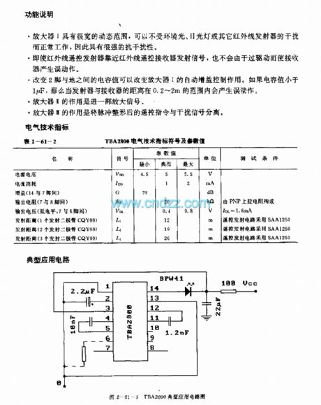
The T6A2800 is designed as the infrared remote control receiving bipolar type circuit that can be used in TV application. The internal circuit is composed of the gain control amplifier I, amplifier II, the pulse separation amplifier III and the inverter. The matching models are SAA1250 or IRT1250. It is in the 14-pin dual-row DIP plastic package.
Function declaration
The amplifier I has the wide dynamic range, it will not interfere by the environment light, the fluorescent lamp or other infrared transmitters.
Even if the infrared remote control transmitter closes to the infrared remote control receiver transmitter signal, the receiver will not produce the false action because of the overdrive.
(View)
View full Circuit Diagram | Comments | Reading(1467)
Precision_high_CMV_common_mode_voltage_analog_isolator
Published:2009/7/21 3:00:00 Author:Jessie

Precision high CMV (common mode voltage) analog isolator. This circuit provides up to 1500 volts DC CMV isolation. The V/F convener shown is a 452 with a full scale output of 100 kHz for 10 volts input (courtesy Analog Devices, Inc.). (View)
View full Circuit Diagram | Comments | Reading(751)
0_20_Hz_DATA_DEMODULATOR
Published:2009/7/8 22:58:00 Author:May
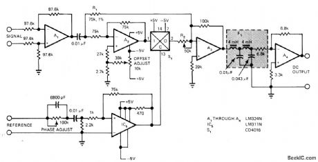
Used for measuring and monitoring suppressed-carriersignal modulation from alrcraft control sys-terms.Provides data frequency response,withhin o.1 dB from DC to 20 Hz,with linearity better than 0.1%. In-phase reference voltage applied to comparator IC5 controls gating of CD4016 MOS switch S1.Suppressed-carrier signal is buffered by opamp A1 for branching to summing junction of A3. Article describes operation of circuit.-J. A. Tabb and M. L. Roginsky, Instrumentation Signal Demodulator Uses LowPower IC's, EDN Magazine, Jan. 20, 1976, p 80. (View)
View full Circuit Diagram | Comments | Reading(620)
TA8141S (TV) infrared remote control receiving circuit
Published:2011/7/27 4:29:00 Author:TaoXi | Keyword: TV, infrared, remote control, receiving circuit
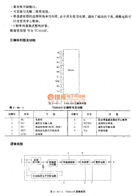

The TA8141S is designed as one kind of infrared remote control receiving bipolar type circuit that can be used in the TV application. The internal circuit is composed of the preamplifier single circuit, the ABLC circuit, the amplitude limiting amplifier circuit, the bandpass filter, the wave detector and the shaping circuit.
Features
Low current consumption. When the power supply voltage is 5V, the operating current is 2mA.This circuit has the band-pass filter, and you do not need to adjust the band-pass filter (BPF).The collector electrode is in the open-circuit output state.It can be connected with the photodiode directly.The frequency-selective network of the band-pass filter uses the resistance.9-pin single row DIP plastic package.The matching model is TC9012F.
(View)
View full Circuit Diagram | Comments | Reading(1032)
AC_RELAY
Published:2009/7/8 22:54:00 Author:May
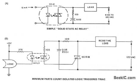
When zero voltage switching is not required, methods of providing this function are illustrated. The lowest parts count version of a solid-state relay is an optoisolator, the triac driver H11J. Unfortunately, the ability of the H11J to drive a load on a 60-Hz line is severely limited by its power dissipation and the dynamic characteristics of the detector. These factors limit applications to 30 - 50 mA resistive loads on 120 Vac, and slightly higher values at lower voltages. These values are compatible with neon lamp drive, pilot, and indicator incandescent bulbs; low voltage control circuits, such as furnace and bell circuits, if dV/dt are sufficient; but less than benign loads require a discrete triac.
The H11J1 triac trigger optocoupler potentially allows a simple power switching circuit utilizing only the triac, a resistor, and the optocoupler. This configuration will be sensitive to high values of dV/dt and noise on normal power-line voltages, leading to the need for the configuration shown in Fig. 67-14B, where the triac snubber acts as a filter for line voltage to the optocoupler.
Since the snubber is not usually used for resistive loads, the cost effectiveness of the circuit is compromised somewhat. Even with this disadvantage, the labor, board space, and inventory of parts savings of this circuit prove it cost-optimized for isolated logic control of power-line switching. In applications where transient voltages on the power line are prevalent, provisions should be made to protect the H11J1 from breakover triggering. (View)
View full Circuit Diagram | Comments | Reading(1146)
TA7344P general remote control receiving preamplifier circuit
Published:2011/7/27 19:11:00 Author:TaoXi | Keyword: general, remote control, receiving, preamplifier circuit


The TA7344P is designed as the general remote control receiving preamplifier circuit. The internal circuit is composed of the preamplifier circuit, the peak value detection circuit, the voltage stabilization circuit, the waveform plastic loop. It is in the 9-pin single row DIP package.
(View)
View full Circuit Diagram | Comments | Reading(761)
QRP_CW_TRANSCEIVER
Published:2009/7/8 22:54:00 Author:May

This is a 3-W, single-circuit board, VFO-controlled CW transceiver for 40 or 30 me'ers, featuring a direct-conversion receiver with audio filtering, Receiver Incremental Tuning (RIT). and speaker level audio volume. The transmit frequency is generated by Q1 and its associated component in the VFO The buffer, Q2, isolates the oscillator from the other circuitry to help the VFO stable.Q3 builds up the signal to a more usable level. The driver, Q4, amplifies the signal. The final, Q5, amplifies it to the 3-W level.Key the transmitter by turning the power to the driver on and off using Q6 as a switching transistors Selec.the frequency by varying the,tuning capadtor, C2. The VFO frequency feeds into the diode-ring mixer, and is mixed with the incoming 7-or 10-MH, signal. The difference or produce,is the audio frequency. The post-mixer circuitry amplifies the audio sianal to speaker leve Q8 preamplifies the signal a little, U2 is an audio filter that attenuates the audio signals above about 700 Hz, and U3 amplifies the signal from the audio filter to listening level. (View)
View full Circuit Diagram | Comments | Reading(2589)
| Pages:929/2234 At 20921922923924925926927928929930931932933934935936937938939940Under 20 |
Circuit Categories
power supply circuit
Amplifier Circuit
Basic Circuit
LED and Light Circuit
Sensor Circuit
Signal Processing
Electrical Equipment Circuit
Control Circuit
Remote Control Circuit
A/D-D/A Converter Circuit
Audio Circuit
Measuring and Test Circuit
Communication Circuit
Computer-Related Circuit
555 Circuit
Automotive Circuit
Repairing Circuit