
Circuit Diagram
Index 923
CASCODE_RF_AMPLIFIER
Published:2009/7/9 1:23:00 Author:May
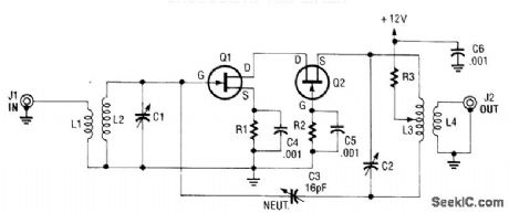
A cascode amplifier using two MOSFETs is shown in the diagram. L2C1 and L3C2 resonate to the frequency in use. The circuit has the advantage of good gain, low NF, and excellent linearity. Q1 and Q2 can be MPF102 or 2N4416. (View)
View full Circuit Diagram | Comments | Reading(2036)
NO_CALIBRATION_OHMMETER
Published:2009/7/20 20:54:00 Author:Jessie
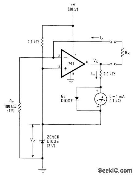
When unknown resistor RX is connected, milliammeter reading is RX/RC where RC is value of known standard resistor used. RX is then equal to meter reading in milliamperes multiplied by value of RC in ohms. Full-scale deflection is thus obtained on 1-mA meter when RX is 100K. Other ranges can be obtained by changing value of RC, using range switch if desired. Meter has automatic zeroing because VO rises to exactly 3 V when measuring leads are shorted and no current flows through meter.-V. Ramprakash, Direct-Reading Ohmmeter Needs No Calibration, Electronics, Nov, 11, 1976, p 115-116. (View)
View full Circuit Diagram | Comments | Reading(695)
RLC_OSCILLATOR
Published:2009/7/9 1:23:00 Author:May

A positive transient, such as the power switch closing, charges C through L to a voltage above the supply voltage, if Q is sufficient. When the current reverses, the diode blocks and triggers the SCS. As the capacitor discharges, the anode gate approaches ground potential, depriving the anode of holding current. This turns off the SCS, and C charges to repeat the cycle. (View)
View full Circuit Diagram | Comments | Reading(700)
CLAMPED_SYNC_SEPARATOR
Published:2009/7/20 20:53:00 Author:Jessie
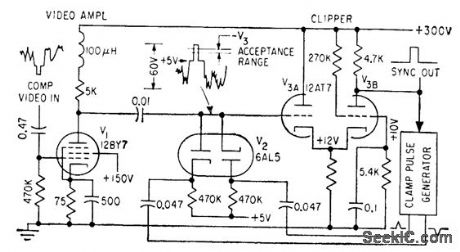
Separates sync from composite input signal at studio, for automatic video level control.-J. O. Schroeder, Holding Video Levels While Switching Studios, Electronics, 32:22, p 96-98.
(View)
View full Circuit Diagram | Comments | Reading(448)
VIDEO_LINE_DRIVING_AMPLIFIER
Published:2009/7/9 1:22:00 Author:May

Q1 and Q2 form a differential stage which single-ends into the LT1010. The capacitively terminated feedback divider gives the circuit a dc gain of 1, while allowing ac gains up to 10. Using a 20-Ω bias resistor, the circuit delivers 1 V pk-pk into a typical 75-Ω video load. For applications sensitive to NTSC requirements, dropping the bias resistor value will aid performance. At A = 2, the gain is within 0.5 dB to 10 MHz and the -3 dB point occurs at 16 MHz. At A = 10, the gain is flat, with ±0.5 dB to 4 MHz .and the -3 db point occurs at 8 MHz。The peaking adjustment should be optimized under loaded output conditions. (View)
View full Circuit Diagram | Comments | Reading(1035)
RECORDING_MANOMETER
Published:2009/7/20 20:49:00 Author:Jessie

Pressure of blood or other body liquids is measured and recorded by photoelectric system.Mercury or other opaque fluids may also be measured. Servo loop maintains photocell at meniscus level of liquid,Mechanicallinkagealso drives recorder stylus,-W. E. Gilson and H.Ludwig, Recording Manometer Electronics,32:52,p 41. (View)
View full Circuit Diagram | Comments | Reading(564)
SLOW_SCAN_TV_RECEIVER
Published:2009/7/20 20:48:00 Author:Jessie

Signals from f-m telemetry system in balloon are picked up by commercial receiver and fed to distribution amplifier serving three monitors, having identical circuits as shown. Video band-width is 200 kc.-L. E. Flory et al., Television System for Stratoscope I, Electronics, 33:25, p 49-53.
(View)
View full Circuit Diagram | Comments | Reading(1496)
FIXED-FREQUENCY_VARIABLE_DUTY_CYCLE_OSCILLATOR
Published:2009/7/9 1:21:00 Author:May

In a basic astable timer,configuration periods t1 and t2 are not controlled independently. The lack of control make it difficult to maintain a constant period,T,if either t1 or t2 is varied.In this circuit,charge RAB and discharge RBC resistance are determined by the position of common wiper arm B of the Potentiometer so,it is possible to adjust the duty-cycle by adjusting t1 and t2 Proportionately,without changing period T.
At start-up,the voltage across G is less than the trigger level voltage (1/2 VDD),causing the timer to be triggered via pip 2,The output of the timer at m 3 Increases,turning off the discharge transistor at pin 7 and allowina Ct to charge through diode D1 and resitance RAB.When capacitor Ct charges to upper threshold voltage 2/3 VDD,the flip-flop is reset and the output at pin 3 decreases through diode D2 and resistor RBC.When the voltage at pin 2 reaches 1/3 VDD,the lower threshold or trigger level,the timer triggers.again and the cycle is repeated.In this circuit,the oscillator frequency remains fixed and the duty cycle is adjustable from less than 0.5% to greater than 99.5%. (View)
View full Circuit Diagram | Comments | Reading(1254)
Shunt_regulator+5_voltsusing_an_ECG915_or_ECG915D
Published:2009/7/20 20:48:00 Author:Jessie
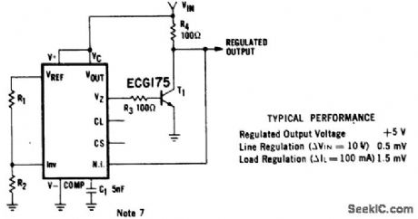
Shunt regulator(+5 volts)using an ECG915 or ECG915D.For a ±5% fixed output resistor R1 is 2.15 ohms and R2 is 4.99 ohms,For metal can applications where Vz is required,a 6.2-volt zener should be connected in series with the regulated output(courtesy GTE Sylvania Incorporated). (View)
View full Circuit Diagram | Comments | Reading(463)
VARACTOR_TUNED_PRESELECTOR
Published:2009/7/9 1:20:00 Author:May
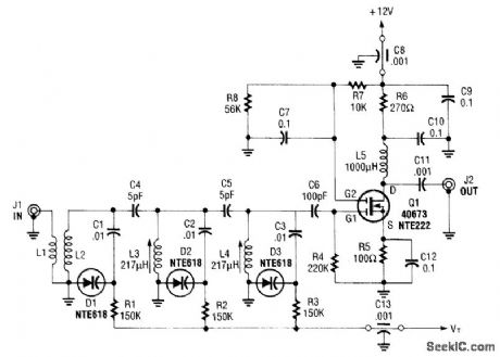
Varactor diodes replace the conventional 365-pF tuning capacitors, which reduces size and weight when used as a turned RF stage for AM broadcast applications. Selectivity is good enough for use as a TRF receiver if a detector is connected to J2. (View)
View full Circuit Diagram | Comments | Reading(1072)
Multicrystal_RF_oscillator_for_the_100_kHz_to_20_MHz_range
Published:2009/7/20 23:46:00 Author:Jessie

Multicrystal RF oscillator for the 100 kHz to 2.0 MHz range (courtesy Motorola Semiconductor Products Inc.). (View)
View full Circuit Diagram | Comments | Reading(647)
BROADCAST_BAND_BOOSTER
Published:2009/7/9 1:19:00 Author:May
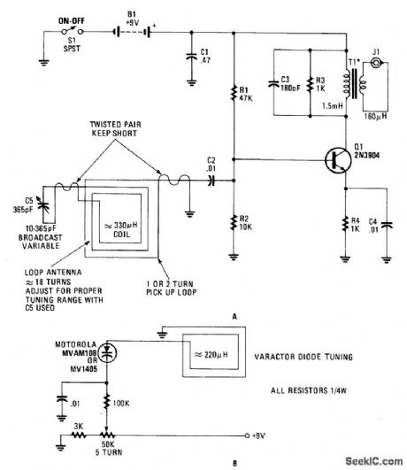
The use of a loop antenna oflarge size (12×18″)provides a large signal pickup at AM broadcast frequencles.It has about 18 turns. T1 is a toroidal transformer of about⒊1 turns ratio (not critical).Theprimary winding should have about 1.5 mH inductance. By using the circuit at (B),a varactor diode can beused In place of the 10- to 365-pF variable capacitor. (View)
View full Circuit Diagram | Comments | Reading(889)
MODULATOR_TRANSFORMER
Published:2009/7/20 23:47:00 Author:Jessie
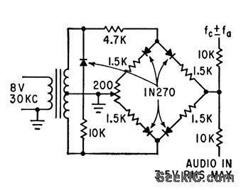
Circuit provides best possible balance between halves of center-tapped secondary, as required for precise phase splitting, in Boynton-Scholt modulator shown.-Wide-Band Transformer Covers 3 Kc to 22 Mc, Electronics, 35:25, p 66. (View)
View full Circuit Diagram | Comments | Reading(539)
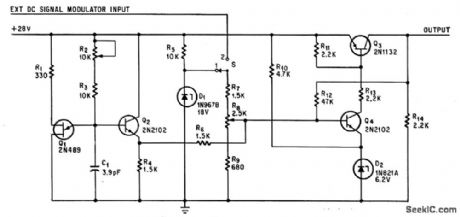
DIAMOND_MODULATOR
Published:2009/7/20 23:48:00 Author:Jessie

Carrier signal turns electron tube or equivalent crystal diode on and off to modulate d-c input signal. Signal-noise ratio is about 1,500 to 1, with carrier voltage of 19V rms. Output is linear up to 3 V rms for d-c inputs up to 10 V.-L. S.Klivans, Modulators for Automatic Control Systems, Electronics, 31:1, p 82-84. (View)
View full Circuit Diagram | Comments | Reading(573)
DIRECT_R_C_COUPLED_COMMON_EMITTER_MODULATOR
Published:2009/7/20 23:50:00 Author:Jessie

Performance is considerably better than that of conventional trans. former-coupled collector-modulated 27-Mc CB modulator. Total current drain is 83 ma.0.14 v gives full modulation. Power gain is nearly 20 db for 2N1193. Requires no audio transformers.-B. Rheinfelder, Modulation Techniques for Transistorized A-M Transmitters, EEE, 11:7, p 54-57. (View)
View full Circuit Diagram | Comments | Reading(537)
PLL_frequency_synthesizer_with_109_MHz_to_12399_MHz_output
Published:2009/7/20 23:52:00 Author:Jessie

PLL frequency synthesizer with 10.9 MHz to 12.399 MHz output. This circuit is designed to generate at 10.7 MHz IF over the 200 kHz to 1699 kHz band for an ADF. Steps are 1 kHz apart (courtesy Motorola Semiconductor Products Inc.). (View)
View full Circuit Diagram | Comments | Reading(3361)
MODEM_PULSE_SHAPER
Published:2009/7/20 23:52:00 Author:Jessie

Removes audio component from modulator output to prevent crosstalk, and shapes pulse to required rise and fall lime and width. Used in four-channel ppm microwave multiplex unit.-P. W. Kiesling, Jr., Portable Multiplexor for Telephone Communications, Electronics, 32:2; p 60-62. (View)
View full Circuit Diagram | Comments | Reading(498)
PWM
Published:2009/7/20 23:54:00 Author:Jessie
With S1 at 1, circuit is unjunction-transistor pulse generator with prf variable from 13 to 25 kc, and duty cycle variable from 0 to 100%. With S1 at 2, circuit is modulator whose output pulse width varies with level of external d-c signal.-D. L. Patillo, Pulse Generator Circuit Doubles Modulator, Electronics, 38:8, p 91-92. (View)
View full Circuit Diagram | Comments | Reading(964)
Voltage_controlled_sine_wave_oscillator
Published:2009/7/20 23:55:00 Author:Jessie

Voltage-controlled sine-wave oscillator. Two AD534 multipliers are used to form integrators with controllable time constants in a second-order differential-equation feedback loop. The waveform shows the VCO's response to a ramp input (courtesy Analog Devices, Inc.). (View)
View full Circuit Diagram | Comments | Reading(0)
300_KW_MAGNETRON_MODULATOR
Published:2009/7/20 23:55:00 Author:Jessie
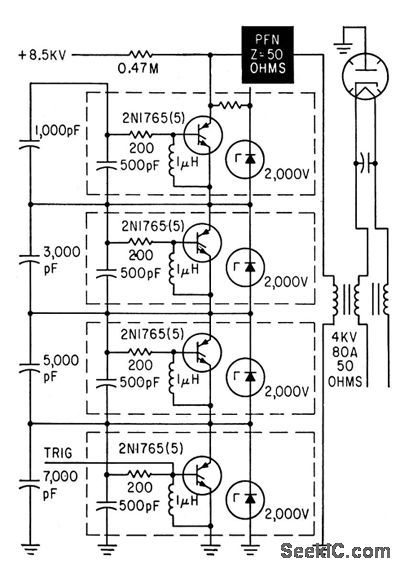
Trigger is applied to first of four 2-kv switch modules arranged in series, for simultaneous triggering of other modules to furnish 16-kv 20-amp pulse to type 7208 Ku-band coaxial magnetron through standard 50-ohm pulseforming network PFN.-F. A. Gateka and M. L.Embree, Semiconductor Modulators for Modern Magnetrons, Electronics, 35:37, p 42-45. (View)
View full Circuit Diagram | Comments | Reading(1233)
| Pages:923/2234 At 20921922923924925926927928929930931932933934935936937938939940Under 20 |
Circuit Categories
power supply circuit
Amplifier Circuit
Basic Circuit
LED and Light Circuit
Sensor Circuit
Signal Processing
Electrical Equipment Circuit
Control Circuit
Remote Control Circuit
A/D-D/A Converter Circuit
Audio Circuit
Measuring and Test Circuit
Communication Circuit
Computer-Related Circuit
555 Circuit
Automotive Circuit
Repairing Circuit