
Circuit Diagram
Index 925
XY_RECORDER_SERVO
Published:2009/7/21 1:24:00 Author:Jessie
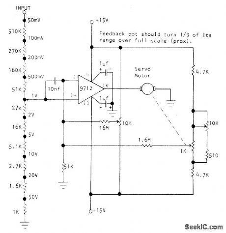
Optical Electronics 9712 FET opamp drives 10-V 0.2-A servomotor used for positioning pen of XY recorder. Circuit provides coarse and fine attenuation of input signal along with position-control pot. FET input of opamp allows use of 1-megohm input attenuator. Response time is limited only by that of servomotor and mechanical portion of system. Requires highly stable regulated power supply.- The 9712 as a Servo Motor Amplifier, Optical Electronics, Tucson, AZ, Application Tip 10206. (View)
View full Circuit Diagram | Comments | Reading(1043)
50DUTY_CYCLE_OSCILLATOR
Published:2009/7/9 1:34:00 Author:May


Frequency of oscillation depends on the R1/C1 time constant and allows frequency adjustment byvarylng R1. (View)
View full Circuit Diagram | Comments | Reading(730)
SCRATCH_FILTER
Published:2009/7/9 1:34:00 Author:May

Designed to produce 12-dB/octave roll-off above the 10-kHz cutofffrequency, this LP active filter will help reduce needle scratch on records. It uses an LM387low-noise amplifier IC. (View)
View full Circuit Diagram | Comments | Reading(0)
HCU_HCT_BASED_OSCILLATOR
Published:2009/7/9 1:33:00 Author:May


When frequency stability is not of prime importance, a simple, yet retable, digital clock oscillator can be made with the aid of relatively few components. High-speed CMOS (HCU/HCT) inverters or gates with an inverter function are eminently suitable to make such oscillators, thanks to their low power con-sumption, good output signal definition, and extensive frequency range.
The circuit as shown uses two inverters in a 74HCT04 or 74HCU04. The basic design equations are:
With RS and R calculated for a given frequency and value of C, both resistors can be realized as presets to enable precise setting of the output frequency and the duty factor. Do not forget, however, to fit small series resistors in series with the presets, in observance of the minimum values for R and RS as given in the design equations. The values quoted for IC are only valid if the inputs of the remaining gates are g fillnded.
(View)
View full Circuit Diagram | Comments | Reading(1298)
DC_GAIN_CONTROLLED_VIDEO_AMPLIFIE
Published:2009/7/9 1:32:00 Author:May
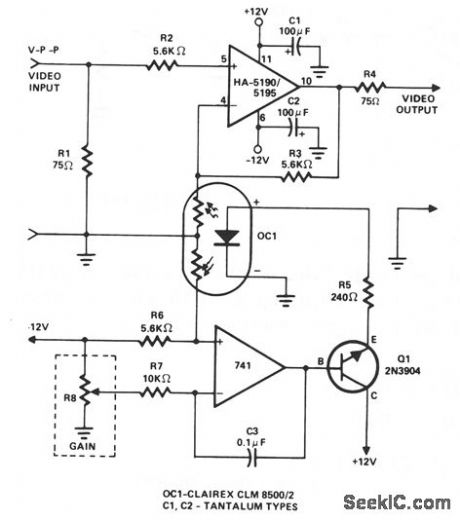
This amplifier employs a cascaded op amp inte-grator and transistor buffer, Q1, to drive the gain control element. Except for a simple modification, the HA-5190/5195 stage is connected as a conven-tional noninverting op amp, and includes input and output impedance matching resistors RI and R4, respectively, series stabilization resistor R2, and power supply bypass capacitors C1 and C2. The circuit differs from standard designs in that the gain control network includes a photoresistor, part of OC1. The optocoupler/isolator OC1 contains two matched photoresistors, both activated by a common LED. The effective resistances offered by these devices are inversely proportional to the light emitted by the LED. One photoresistor is part, with R3, of the HA-5190/5195 gain network, while the other forms a voltage-divider with R6 to control the bias applied to the integrator noninverting terminal.In operation, the dc voltage supplied by gain control R8 is applied to the integrator inverting input terminal through input resistor R7. Depending on the relative magnitude of the control voltage, the integrator output will either charge or discharge C3. This change in output, amplified by Q1, con-trols the current supplied to the OC1 LED through series limiting resistor R5. The action continues until the voltage applied to the integrator noninverting input by the R6-photoresistor gain network is changing, adjusting the op amp stage gain. As the control voltage at R8 is readjusted, the OC1 photoresistances track these changes, automatically readjusting the op amp in accordance with the new control voltage setting. (View)
View full Circuit Diagram | Comments | Reading(976)
2_METER_RECEIVER_CALIBRATOR
Published:2009/7/21 2:08:00 Author:Jessie
Checks both frequency and sensitivity of amateur FM receiver Starts with 3-MHz crystal and provides markers every 30 kHz or every 300 kHz Energy levels are so low that only simple 100-ohm attenuator is needed. Article covers construction and calibration. CR9-CR12 are silicon rated 200 PIV at 500mA, such as HEP156 DS2 is 117-V neon T2 is 12V at 0.3A.-H.Lukoff.A 2-Meter Frequency and Sensitivity Calibrator,QST,Feb,1976,p34-36. (View)
View full Circuit Diagram | Comments | Reading(687)
TWIN_TEE_TONE_OSCILLATOR
Published:2009/7/21 2:09:00 Author:Jessie

A 2N2222 transistor is used in a twin-tee oscillator, followed by a FET buffer circuit. (View)
View full Circuit Diagram | Comments | Reading(1365)
Balance_differential_amplifier_with_a_controlled_constant
Published:2009/7/21 2:09:00 Author:Jessie

Balance differential amplifier with a controlled constant-current-souroe drive and AGC capability. Operation can be from DC to 120 MHz. Supply voltage is typically 9 to 12 volts (courtesy GTE Sylvania Incorporated). (View)
View full Circuit Diagram | Comments | Reading(530)
Percent_of_deviation_ratio_computer
Published:2009/7/21 2:09:00 Author:Jessie

Percent of deviation ratio computer (courtesy Analog Devices, Inc.). (View)
View full Circuit Diagram | Comments | Reading(564)
One_out_of_four_data_selector_using_MC1545G_wide_band_amplifiers
Published:2009/7/21 2:10:00 Author:Jessie
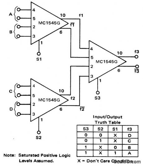
One-out-of-four data selector using MC1545G wide-band amplifiers. This circuit can be modified to be a one-out-of-N data selector (courtesy Motorola Semicon-ductor Products Inc.). (View)
View full Circuit Diagram | Comments | Reading(540)
UJT_OSCILLATOR
Published:2009/7/21 2:11:00 Author:Jessie

When power is connected to the circuit, C1 charges through R1 and R3. When the voltage reaches the UJT gate's (G) threshold voltage (usually around 0.5 to 0.8 of the supply voltage), the dynamic resistance between B2 and B1 drops to a very low value. Capacitor C1 then discharges through the emitter-base junction and the 8-Ω speaker. The frequency of the UJT oscillator is determined by the values of C1, R1, and R3. (View)
View full Circuit Diagram | Comments | Reading(812)
NE602_HARTLEY_VFO_CIRCUIT
Published:2009/7/21 2:12:00 Author:Jessie

In this circuit, L1 is tapped at about one-third to one-fourth from the ground end. L1 is about 10/f MHz, while C1 is chosen to resonate L1 to the desired frequency. (View)
View full Circuit Diagram | Comments | Reading(1334)
VOLTAGE_CONTROLLED_AMPLIFIER
Published:2009/7/9 1:32:00 Author:May
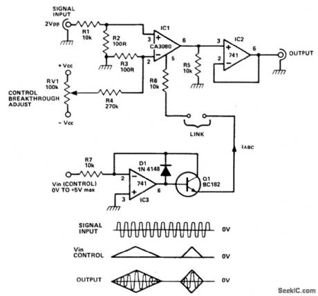
The CA3080 can be used as a gain controlling device. The input signal is attenuated by R1/R2 so that a 20-mVpp signal is applied to the input terminals. If this voltage is much larger, significant distortion will occur at the output. In fact, this distortion is put to good use in the triangle-to-sine wave converter.
The gain of the circuit is controlled by the magnitude of the current IABC. This current flows into the CA3080 at pin 5, which is held at one diode voltage drop above the - VCC rail. The gain of the CA3080 is linearly proportional to the magnitude of the IABC current over a range of 0.1μA to 1 mA. Thus, by controlling IABC, you can control the signal level at the output. The output is a current output, which has to be dumped into a resistive load (R5) to produce a voltage output. The output impedance at IC1 pin 6 is 10 kΩ (R5), but this is unloaded by the voltage follower (IC2) to produce a low output impedance.
The circuit around IC3 is a precision voltage-to-current converter and this can be used to generate IABC. When Vin (control) is positive, it linearly controls the gain of the circuit. When it is negative, IABC is zero and so the gain is zero. (View)
View full Circuit Diagram | Comments | Reading(0)
Fuda Brand ZL130-81 Dry And Wet Vacuum Cleaner Circuit
Published:2011/8/2 22:05:00 Author:Robert | Keyword: Fuda, Dry, Wet, Vacuum Cleaner

The picture shows the Fuda Brand ZL130-81 dry and wet vacuum cleaner circuit.
The XP is power plug. The S is power switch. The FU is fuse. The T is power transformer. The K1 is relay. The K1-1 is relay K1's normally openning contactor. The IC is integrated circuit. The VT is triode. The SP is air pressure sensor. The XT is terminal board. The M is motor. The VD1, VD2are indication lamps. (View)
View full Circuit Diagram | Comments | Reading(2861)
Full_wave_synchronous_rectification_circuit
Published:2009/7/21 2:12:00 Author:Jessie
Full-wave synchronous rectification circuit (courtesy Motorola Semiconductor Products Inc.). (View)
View full Circuit Diagram | Comments | Reading(663)
SECOND_ORDER_100_Hz_HIGH_PASS_FILTER
Published:2009/7/9 1:32:00 Author:May

This second-order filter can be scaled change the cutoff frequencies. (View)
View full Circuit Diagram | Comments | Reading(847)
WIDE_RANGE_OSCILLATOR
Published:2009/7/9 1:31:00 Author:May

The gain control allows the oscillator to maintain essentially constant output over its range. The circuit functions over 160 kHz to 12 MHz with essentially constant amplitude. (View)
View full Circuit Diagram | Comments | Reading(1625)
WIDEBAND_AMPLIFIER_1
Published:2009/7/9 1:31:00 Author:May

This wideband amplifier uses a MARI IC, which is a gain block. The device is manufactured by Mini-Circuits Lab and offers +13-dB gain from dc to 1000 MHz. R1 is selected to provide 17-mA current to UI at +5 V. For 12-V supply R1 = 470 Ω. RFC1 is typically 1 to 5 pH. (View)
View full Circuit Diagram | Comments | Reading(699)
HARTLEY_OSCILLATOR
Published:2009/7/21 2:13:00 Author:Jessie

The oscillator's operating frequency is determined by the values of L1 and C3. The feedback level is determined by the location of the tap on L1, which normally will be about one-fifth to one-fourth of the total turns. As an example, the Hartley oscillator will operate in the 5-MHz range with the following LC values: L1 is 20 turns of 18 enameled copper wire close wound on a 1-inch plastic form with a tap up five turns from the bottom. Capacitor C3 can be any small variable capacitor with a maximum capacitance value of 100 pF. With the proper LC values, the Hartley oscillator can operate from audio to UHF. (View)
View full Circuit Diagram | Comments | Reading(0)
Meiri 3-Cylinder Engine Joint Electronic Control System Circuit
Published:2011/8/3 7:32:00 Author:Robert | Keyword: Meiri, 3-Cylinder, Engine, Joint, Electronic, Control, System
The picture shows the Meiri 3-cylinder engine joint electronic control system circuit.
In the circuit the part 1 is engine. The part 2 is battery. The part 3 is starting machine. The part 4 is ignition switch. The part 5 is speaker. The part 6 is cassette player. The part 7 is relay. The part 8 is electronic clock. The part 9 is oil pump. The part 10 is ECU. The part 11 is canister control valve. The part 12 is oil injector. The part 13 is hall sensor. The part 14 is stepper motor. The part 15 is thermistor. The part 16 is oxygen sensor. The part 17 is ignition coil. The part 18 is cooling fluid temperature sensor. The part 19 is vacuum sensor. The part 20 is throttle position sensor. The 21 is knock sensor. The part 22 is fault diagnosis interface. The part 23 is temperature control switch. The part 24 is fog lamp switch. And so on. (View)
View full Circuit Diagram | Comments | Reading(527)
| Pages:925/2234 At 20921922923924925926927928929930931932933934935936937938939940Under 20 |
Circuit Categories
power supply circuit
Amplifier Circuit
Basic Circuit
LED and Light Circuit
Sensor Circuit
Signal Processing
Electrical Equipment Circuit
Control Circuit
Remote Control Circuit
A/D-D/A Converter Circuit
Audio Circuit
Measuring and Test Circuit
Communication Circuit
Computer-Related Circuit
555 Circuit
Automotive Circuit
Repairing Circuit