
Circuit Diagram
Index 936
Kyocera KZ820 phone cable circuit diagram
Published:2011/8/3 2:01:00 Author:Ecco | Keyword: Kyocera phone cable circuit diagram

View full Circuit Diagram | Comments | Reading(730)
1_OF_8_OHANNEL_TRANSMISSION_SYSTEM
Published:2009/7/8 21:59:00 Author:May
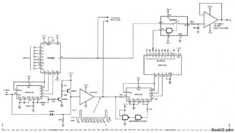
This circuit shows a typical multiplex system intended to carry one of 8 inputs into a remote location.A 5-V pulse train is sent down a separate channel to perform timing and synchronizing functions. A 15-V reset pulse is superimposed on the 5-V clock, which is detected by the MM74C00 in the receiver. Using this system, many remote points can be monitored, one at a time, at any of several locations. (View)
View full Circuit Diagram | Comments | Reading(1053)
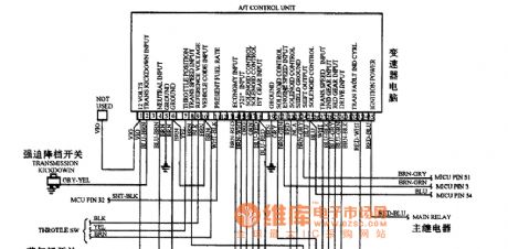
BMW8 Series of EGS 35pin (4HP-22/24) transmission circuit diagram 2
Published:2011/8/3 2:22:00 Author:Ecco | Keyword: BMW8 Series , EGS 35pin transmission
View full Circuit Diagram | Comments | Reading(519)
ADJUSTABLE_GAIN_WIDEBAND_AMPLIFIER
Published:2009/7/8 21:58:00 Author:May
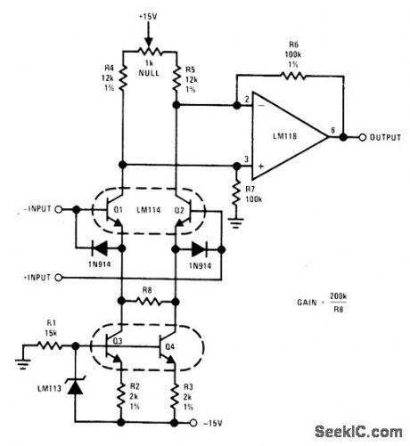
Single resistor R8 adjusts gain from less than1 to over 1000, with gain value equal to 200,000 divided by value in ohms used for R8 Commonmode rejection ratio is about 100 dB, independent of gain. Q1-Q2 are operated open-loop as floating differential input stage. Current sources Q3 and Q4 set operating current of input transistors.- Linear Applications, Vol.2, National Semiconductor, Santa Clara, CA, 1976, LB-21. (View)
View full Circuit Diagram | Comments | Reading(745)
DEMULTIPLEXER
Published:2009/7/8 21:56:00 Author:May

This circuit reconstructs and separates analog signals which have been time-division multiplexed. The conventional method, shown on the left, has several restrictions, particularly when a short dwell time and a long, accurate hold time is required. The capacitors must charge from a low-impedance source through the resistance and current-limiting characteristics of the multiplexer. When holding, the high-impedance lines are relatively long and subject to noise pickup and leakage. When FET input buffer amplifiers are used for low leakage applications, severe temperature offset errors are often introduced. (View)
View full Circuit Diagram | Comments | Reading(2578)
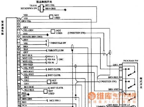
BMW5 Series of 35-pin transmission circuit diagram
Published:2011/8/3 1:54:00 Author:Ecco | Keyword: BMW5 Series , 35-pin transmission
View full Circuit Diagram | Comments | Reading(507)
LOW_COSR_FOUR_CHANNEL_MULTIPLEXER
Published:2009/7/8 21:55:00 Author:May

View full Circuit Diagram | Comments | Reading(566)
BMW6 Series of 35-pin transmission circuit diagram
Published:2011/8/3 1:55:00 Author:Ecco | Keyword: BMW6 Series , 35-pin transmission
View full Circuit Diagram | Comments | Reading(453)
FM_SNOOPER
Published:2009/7/8 21:55:00 Author:May

The FM Snooper is an FM transmitter that radiates a continuous wave whose frequency is alteredaccording to the sound waves striking the microphone. An ordinary FM broadcast recelver detects thetransmitter’s output carner. When 9-V battery,B1,is connected,a brief Surge of current flows from the collector to the emitter of Q1,causing an alternating current,shock oscillation in the resonant LC circuit,to flow back and forth between L1 and C5. So,by varying the value of C5,you can tune the oscillations to the exact frequency desired。Although tuning capacitor C5 accounts for the major part of the tuning capacitance,the capacitance between the base and the collector of Q1 has a small,but noticeable,effect on the oscillati frequency. That capacitance,which is known as the junction capacitance,is not a fixed value,but instead vanes when the voltage on the base of the transistor vanes. Sound waves striking the microphone induce a voltage that vanes in time with the sound. That voltage is applied via C1 to the base ofQ1,thereby frequency modulating the transmitter. (View)
View full Circuit Diagram | Comments | Reading(3204)
50_OHM_LINE_DRIVER
Published:2009/7/8 21:54:00 Author:May

CA3100 bipolar MOS opamp operates as high-slew-rate wideband amplifier that provides 18 V P-P into open circuit or 9 V P-P into 50-ohm transmission line. Slew rate is 28 V/μs.- Circuit Ideas for RCA Linear 1Cs, RCA Solid State Division, Somerville, NJ, 1977, p 13. (View)
View full Circuit Diagram | Comments | Reading(2218)
BMW7 Series of 35-pin transmission circuit diagram
Published:2011/8/3 1:56:00 Author:Ecco | Keyword: BMW7 Series , 35-pin transmission
View full Circuit Diagram | Comments | Reading(510)
1_OF_15_CASCADED_VIDEONUX
Published:2009/7/8 21:54:00 Author:May


Two MAX455s can be cascaded to form a 1 of 15 video MUX by connecting the output of one MUX to one of the input channels of a second MUX. Although the two devices are usually close to one another, the output of the first MUX should be terminated to preserve its bandwidth. (View)
View full Circuit Diagram | Comments | Reading(522)
TWO_LEVEL_MULTIPLEXER
Published:2009/7/8 21:52:00 Author:May

When a large number of channels are multiplexed, the outputs of two or more multiplexers can be connected together and each multiplexer sequentially enabled. In the inhibit mode, the multiplexer draws less power and its output and inputs act as open circuits. Theoretically, an infinite number of channels can be accommodated in this way; in practice, the accumulated output capacitance and leakage of many paralleled multiplexers limits the speed and accuracy of the system. A much better method is the two-level multiplex system. The two-level system has a bank of high-speed switches at the output which sequentially switch between the four DG406s. Each DG406 is able to switch during the time the other three are being interrogated. The DG406s contribute leakage and capacitance at the output only, when they are switched on by the DG411-1/4 of the time. The two-level multiplex system is very useful in communications links, high-speed interfacing with comparators, or wherever a large number of channels must be multiplexed at high speeds.
(View)
View full Circuit Diagram | Comments | Reading(1518)
METAL_DETECTOR
Published:2009/7/8 21:51:00 Author:May

Will detect small coin up to about 5 inches underground and larger metal objects at much greater depths. Frequency of search oscillator Tr1- Tr2 depends on values used for three paralleled capacitors, search coil, and metal obiects in vicinity of coil. Mixer Tr3 feeds difference between search oscillator and reference oscillator Tr4-Tr5 to opamp and Tr6 for driving phones or loudspeaker. Article gives construction and adjustment details, including dimensions for search coil. Reference oscillator is set to 625 kHz. C1 is 560 pF, C2 150 pF, and C3 10 pF variable. C2 is used for coarse tuning, and C3 for fine ad justment to get beat note. Diodes are 1N4148. Tr3 is BC308, BCY72, or equivalent, and other transistors are BF238 BC108, or equivalent.-D. E, Waddington, Metal Detector, Wireless World, April 1977, p 45-48. (View)
View full Circuit Diagram | Comments | Reading(0)
DIFFERENTIAL_INPUT_AMPLIFIER
Published:2009/7/8 21:44:00 Author:May
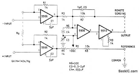
Provides gain up to 1000, depending on value of Rg, for video signals in radar, medical ultrasound,laser communication, and laser rangefinder applications. Uses three Optical Electronics 9906 wideband opamps and 9910 current booster for cable ddve. Bandwidth is above 10 MHz for gains of 0.1 to 100, decreasing to 5 MHz at gain of 1000. Miller compensation of input amplifiers minimizes noise level and gives input impedance of 5 megohms and 5 pF.- Wide Band Instrumentation Amplifier, Optical Electronics, Tucson, AZ, Application Tip 10276. (View)
View full Circuit Diagram | Comments | Reading(1770)
±34_V_COMMON_MODE_RANGE
Published:2009/7/8 21:39:00 Author:May

Interconnections shown for three LM143 high-voltage opamps give equivalent of single differentialinput opamp having wide common-mode range, high input impedance, and gain of 1000.Adjust R2 to trim gain. Adjust R7 for best common-mode rejection. With 10 K load, frequency response is down 3 dB at 8.9 kHz.- Linear Applications, Vol, 2, National Semiconductor, 'OUT Santa Clara, CA, 1976, AN-127, p 2-3. (View)
View full Circuit Diagram | Comments | Reading(752)
LOW_COST_HALF_DUPLEX_INFORMATION_TRANSMISSION_LINK
Published:2009/7/8 21:37:00 Author:May
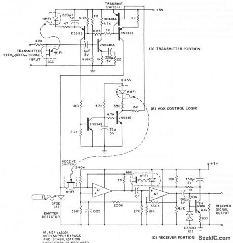
In a half-duplex system, information can flow in both directions, but only one direction at any given time. The conventional method of building a half-duplex link requires a separate emitter and detector, connected with directional couplers, at each end of the fiber. The GFOEIA series of infrared emitting diodes are highly efficient, long-lived emitters, which are also sensitive to the 940 nm infrared they produce. Biased as a photodiode, they exhibit a sensitivity of about 30 nA per μW irradiation at 940 nm. In a suitable bias and switching logic network, they form the basis for a half-duplex information link. A half-duplex link, illustrating the emitter-detector operation of the GFOE1A1, is shown.This schematic represents a full, general purpose system, including: approximately 50-dB compliance range with 1-V rms output, passive receive, voice-activated switching logic, 100 Hz to 50 kHz frequency response, and inexpensive components and hardware. The system is simple, inexpensive, and can be upgraded to provide more capability through use of higher gain bandwidth amplifier stages. Conversely, performance and cost can be lowered simply by removing undesired features. (View)
View full Circuit Diagram | Comments | Reading(1126)
STRAIN_GAGE_AMPLIFIER
Published:2009/7/8 21:33:00 Author:May
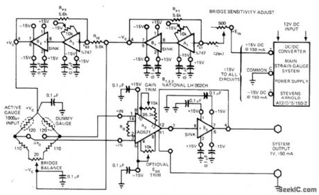
Optimum performance is achieved in fully portable system by utilizing combination of 747 opamps for A1 and A2 with National LH002CH opamp for B1-B3 and special AD521K instrumentation amplifier for output stage. Bypass capacitors suppress undesirable high-frequency signals. Stevens-Arnold DC/DC converter operating from 12-V storage battery provides required regulated ±15 VDC for system while giving excellent power isolation.-D. Sheehan, Strain-Gauge Transducer System Uses Off-the-Shelf Components, EDN Magazine, Nov. 5, 1977, p 79-81.
(View)
View full Circuit Diagram | Comments | Reading(2616)
1_W_CW_TRANSMITTER
Published:2009/7/8 21:31:00 Author:May
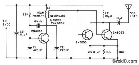
This is a little transmitter that could be put into a plastic Easter egg. It delivers approximately 1 W of measured rf output into a 50-Ω dummy load, and creates no heating problems with the circuit. The crystal is a series fundamental type, and the power source provides 9 V with a 2-A supply. The transmitter can operate at another frequency, but C1 and C2 might have to be changed for the circuit to work properly. The secondary of L1 is wound over the center of a 10- μH coil, with five turns of #30 enameled wire. (View)
View full Circuit Diagram | Comments | Reading(1781)
METER_AMPLIFIER
Published:2009/7/8 21:28:00 Author:May

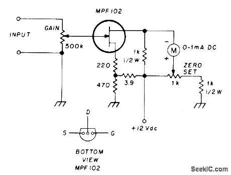
Junction FET in simple DC amplifier circuit converts 0-1 mA DC milliammeter to 0-100μADC microammeter. Adjust zero-set control for zero meter current with no input, then apply input signal and adjust gain to desired value.-N. J. Foot, Electronic Meter Amplifier, Ham Radio, Dec. 1976, p 38-39. (View)
View full Circuit Diagram | Comments | Reading(2948)
| Pages:936/2234 At 20921922923924925926927928929930931932933934935936937938939940Under 20 |
Circuit Categories
power supply circuit
Amplifier Circuit
Basic Circuit
LED and Light Circuit
Sensor Circuit
Signal Processing
Electrical Equipment Circuit
Control Circuit
Remote Control Circuit
A/D-D/A Converter Circuit
Audio Circuit
Measuring and Test Circuit
Communication Circuit
Computer-Related Circuit
555 Circuit
Automotive Circuit
Repairing Circuit